
 EN
EN
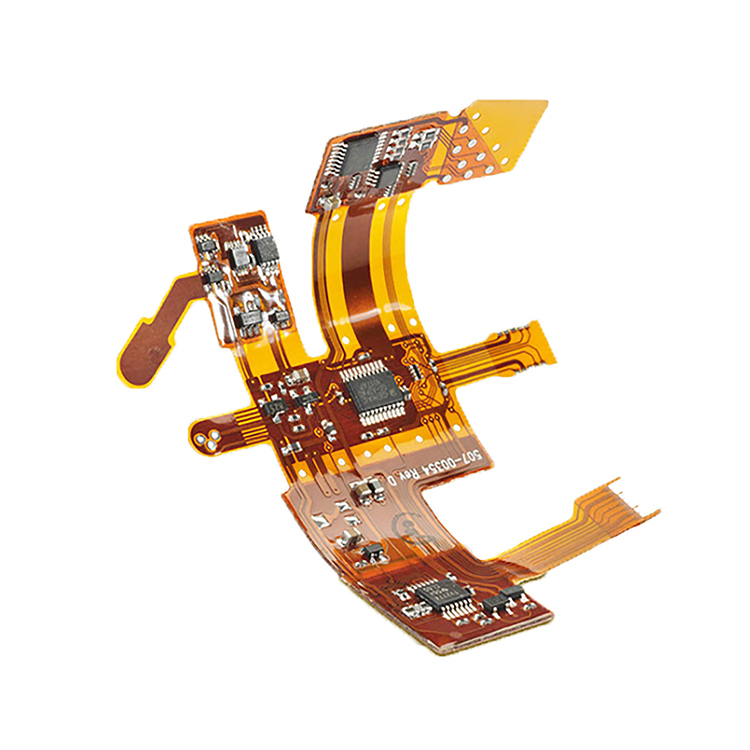
Flexible Printed Circuit Assembly Enables 3D Spatial Optimization
Rigid-flex integration for volume-efficient packaging in space-constrained systems
Rigid-flex integration merges rigid circuit sections with flexible interconnects into a single, three-dimensional assembly—transforming unused enclosure volume into functional real estate. Unlike planar PCBs, rigid-flex circuits fold around batteries, sensors, and mechanical components, reducing total board area by 30–50% while cutting weight significantly. This consolidation eliminates bulky connectors and ribbon cables, simplifying system architecture and improving reliability. The rigid portions maintain structural integrity for component mounting, while flex layers enable dynamic routing in tight spaces. Assembly becomes a single-step process, lowering labor costs, procurement complexity, and interconnect failure risk. For implantable medical devices, compact IoT nodes, and aerospace systems, rigid-flex design turns the third dimension into a strategic advantage—delivering more functionality in smaller, lighter, and manufacturable packages.
Dynamic folding and conformal routing to replace rigid interconnects and reduce planar footprint
Dynamic folding leverages the mechanical compliance of polyimide substrates to route signals along curved paths, through hinges, and across irregular surfaces—replacing planar connectors and cables with a single, integrated flex assembly. Conformal routing allows the circuit to follow the product’s housing contour, enabling installation (and sometimes operation) in folded, twisted, or wrapped configurations. With bend radii as low as six times the foil thickness, flex circuits fit into narrow gaps or wrap around cylindrical enclosures, dramatically shrinking the planar footprint. This approach is essential in foldable smartphones—where assemblies endure hundreds of thousands of dynamic bends—and in wearables that must conform to anatomical contours. By shortening signal paths and removing discrete interconnects, conformal routing also improves signal integrity and reduces electromagnetic interference. The result is thinner, lighter, and more mechanically durable products—without compromising electrical performance.
Material and Interconnect Advancements in Flexible Printed Circuit Assembly
Ultra-thin polyimide substrates and high-density microtrace routing for layer minimization
Polyimide substrates—now available as thin as 12.5 µm—form the backbone of modern flexible printed circuit assembly. When paired with adhesiveless copper cladding, they eliminate bonding layers that add unnecessary thickness and stiffness. This material system directly enables ultra-compact designs where every micron matters.
High-density interconnect (HDI) techniques support microtrace routing with line widths and spaces down to 25 µm, packing more signal pathways into each conductive layer. As a result, complex six-layer rigid PCBs are routinely consolidated into two- or three-layer flex circuits. Fewer layers mean reduced profile, lower mass, and improved signal integrity—particularly critical in high-speed and RF applications. Precision manufacturing methods like laser direct imaging and semi-additive processing ensure consistent yields at these fine geometries. Together, ultra-thin substrates and HDI routing make it possible to embed electronics in spaces previously considered inaccessible.
Bend radius engineering and dynamic flex reliability for compact, moving assemblies
Bend radius is a fundamental design parameter governing flex circuit durability. A minimum static bend radius of ten times the material thickness is standard for single-layer flex; multi-layer constructions require more conservative ratios—typically 20 to 30×—to prevent copper cracking and dielectric delamination.
Dynamic applications—such as printer heads, robotic joints, and hinge mechanisms—pose greater challenges, subjecting circuits to millions of flex cycles. Here, material selection and stack-up design are decisive: rolled annealed copper offers superior fatigue resistance over electrodeposited copper, with elongation up to 20% before failure. Engineers also optimize neutral axis placement by balancing layer symmetry—keeping copper traces in compression rather than tension during bending. Aligning copper grain direction with the primary bend axis further enhances cycle life. When applied rigorously, these principles yield flexible printed circuit assemblies capable of exceeding 100 million dynamic flex cycles—proven reliable in compact, motion-critical systems where rigid interconnects would fail prematurely.
Mechanical Resilience: Stress Management in Miniaturized Flexible Printed Circuit Assembly
As flexible printed circuit assemblies shrink and operate under dynamic bending, thermal cycling, and vibration, mechanical stress concentrates at solder joints, trace corners, and rigid-flex transitions. A 2022 study on rigid-flex PCBs for MEMS pressure sensors confirmed that combined thermal and vibrational loads accelerate solder-joint fatigue—underscoring the need for intentional stress mitigation.
Designers address this with five key strategies:
- Strain-relief loops, strategically placed in flex zones, absorb bending and torsion, diverting stress away from soldered components.
- Adhesive-backed stiffeners, applied at connector interfaces, limit localized flexing and reinforce high-stress attachment points.
- Controlled impedance routing, using gradual trace-width transitions and rounded corners, eliminates sharp stress risers.
- Low-modulus adhesives and coverlay materials, selected for matched CTE and elasticity, accommodate thermal expansion mismatches without delamination.
- Plated through-hole (PTH) reinforcement, including copper-filled vias and optimized annular rings, ensures via integrity under repeated flexure.
Together, these techniques preserve both electrical continuity and mechanical robustness—enabling long-term reliability in miniaturized, high-stress environments.
Real-World Validation: Flexible Printed Circuit Assembly in High-Density Applications
Foldable Smartphones: Hinge-Integrated Dynamic Flex Assemblies Enabling Sub-5mm Fold Volumes
Foldable smartphones rely on dynamic flex assemblies engineered to route signals across moving hinges without signal degradation or mechanical failure. These circuits achieve sub-0.5 mm bend radii while maintaining durability beyond 10,000 flex cycles. According to a 2023 supply chain analysis, leading models now integrate hinge-optimized flex assemblies that reduce total hinge stack thickness to just 4.2 mm—enabling full device folding into a sub-5 mm volume. This spatial efficiency delivers the sleek, pocketable form factors consumers demand, while sustaining high-speed data and power delivery across the fold.
Implantable Medical Devices: Rigid-Flex PCBs Achieving <2mm Cross-Sections with Full Functionality
Implantable devices—including next-generation pacemakers and neurostimulators—demand extreme miniaturization without compromising functionality or longevity. Rigid-flex printed circuit assemblies meet this challenge by integrating rigid component-mounting areas with ultra-thin flexible polyimide layers, eliminating connectors and discrete wiring. Using laser-drilled microvias and stacked dielectric films, engineers compress full sensor, processor, and power management functionality into cross-sections under 1.8 mm. As documented in a 2024 medical electronics report, the latest implantable cardioverter-defibrillators employ rigid-flex assemblies with a 1.6 mm cross-section—housing all critical electronics within the body’s confined anatomical spaces while ensuring safe, long-term in vivo operation.
FAQ
What is rigid-flex integration?
Rigid-flex integration combines rigid circuit sections with flexible interconnects into a single assembly, enabling spatial optimization and reduction of connectors and ribbon cables.
Why are flexible printed circuit assemblies used in foldable smartphones?
These assemblies enable signal routing across hinges while maintaining durability, allowing sleek designs with sub-5mm fold volumes.
What materials are used in flexible printed circuit assemblies?
Ultra-thin polyimide substrates and adhesiveless copper cladding are used to achieve compact designs and high-density interconnect routing for smaller products.
How is mechanical stress managed in miniaturized flexible printed circuits?
Stress management techniques include strain-relief loops, adhesive-backed stiffeners, controlled impedance routing, low-modulus adhesives, and reinforced plated through-holes.
What is the significance of bend radius in flexible circuits?
Bend radius is critical for circuit durability, especially in dynamic applications subjected to millions of flex cycles.
Table of Contents
- Flexible Printed Circuit Assembly Enables 3D Spatial Optimization
- Material and Interconnect Advancements in Flexible Printed Circuit Assembly
- Mechanical Resilience: Stress Management in Miniaturized Flexible Printed Circuit Assembly
- Real-World Validation: Flexible Printed Circuit Assembly in High-Density Applications
-
FAQ
- What is rigid-flex integration?
- Why are flexible printed circuit assemblies used in foldable smartphones?
- What materials are used in flexible printed circuit assemblies?
- How is mechanical stress managed in miniaturized flexible printed circuits?
- What is the significance of bend radius in flexible circuits?

