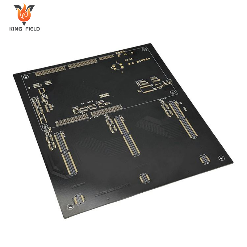
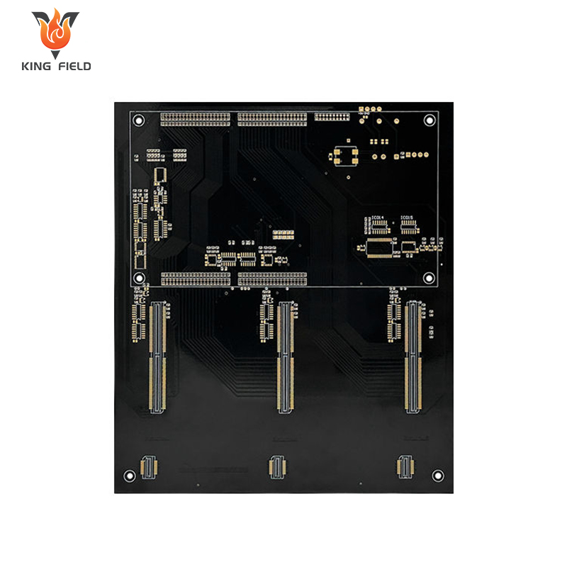
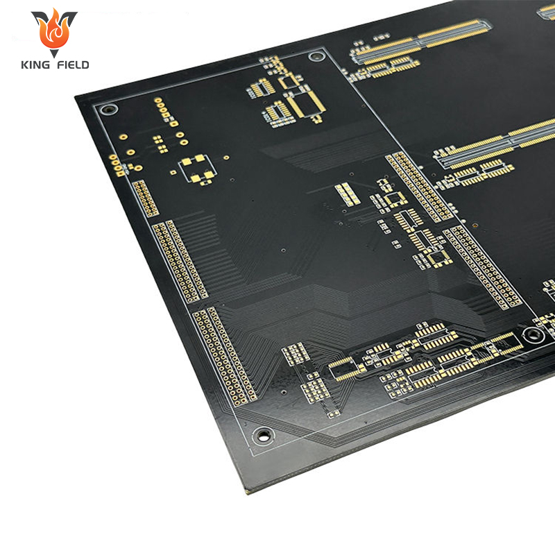
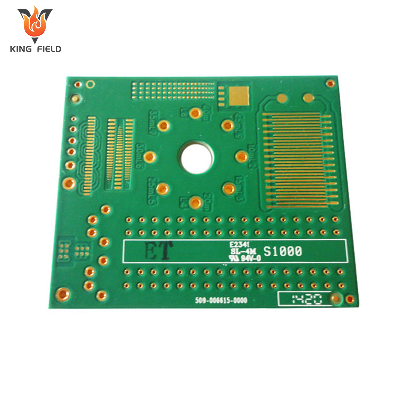
FR4 PCB
As a PCB manufacturer with over 20 years of professional experience, KING FIELD is committed to providing global customers with high-quality, highly reliable FR4 circuit board solutions.
☑ Minimum line width/line spacing 3mil/3mil
☑ Meets UL 94V-0 flame retardant rating
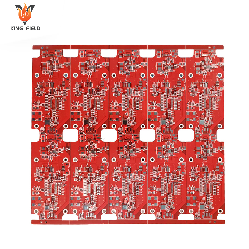
☑ Excellent processing performance; capable of producing 1-100 layer FR4 PCBs.
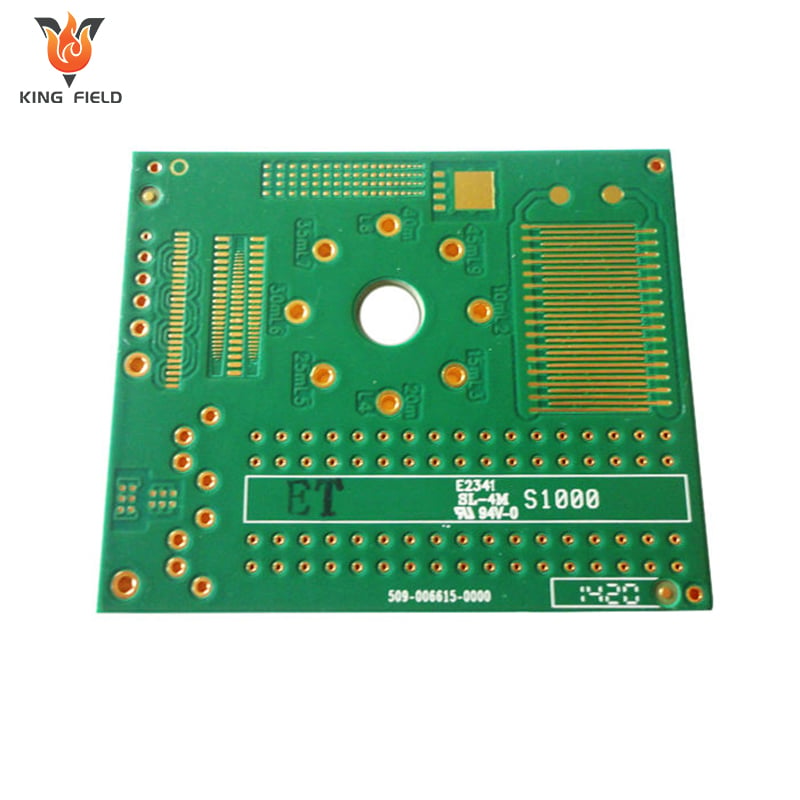
Description
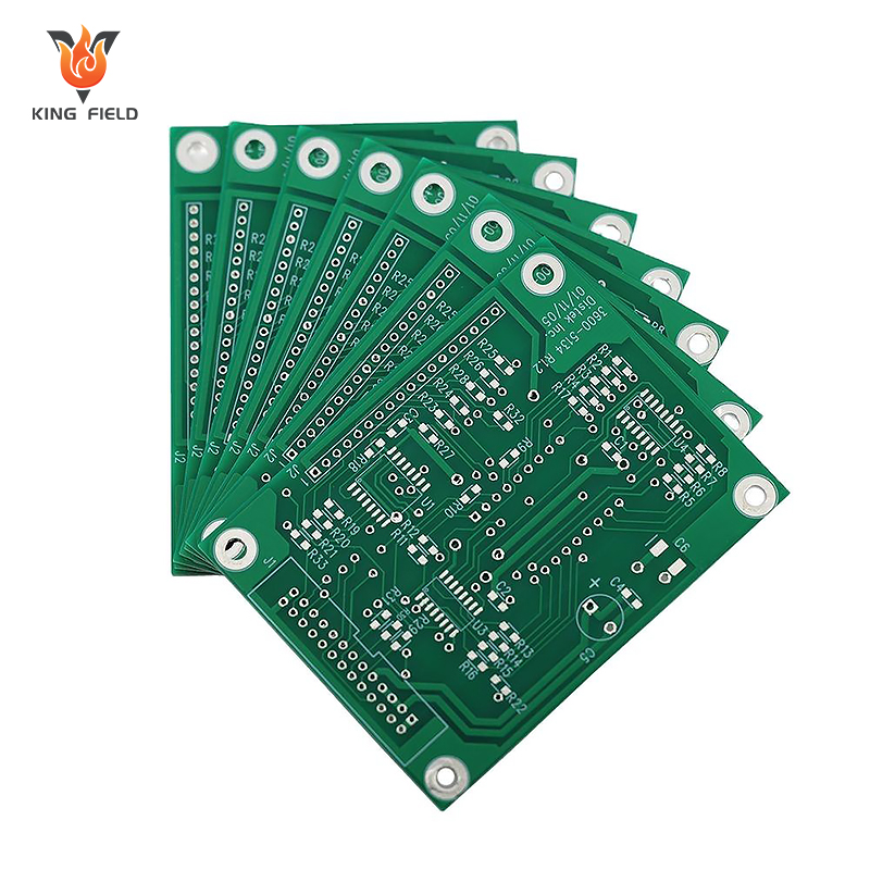
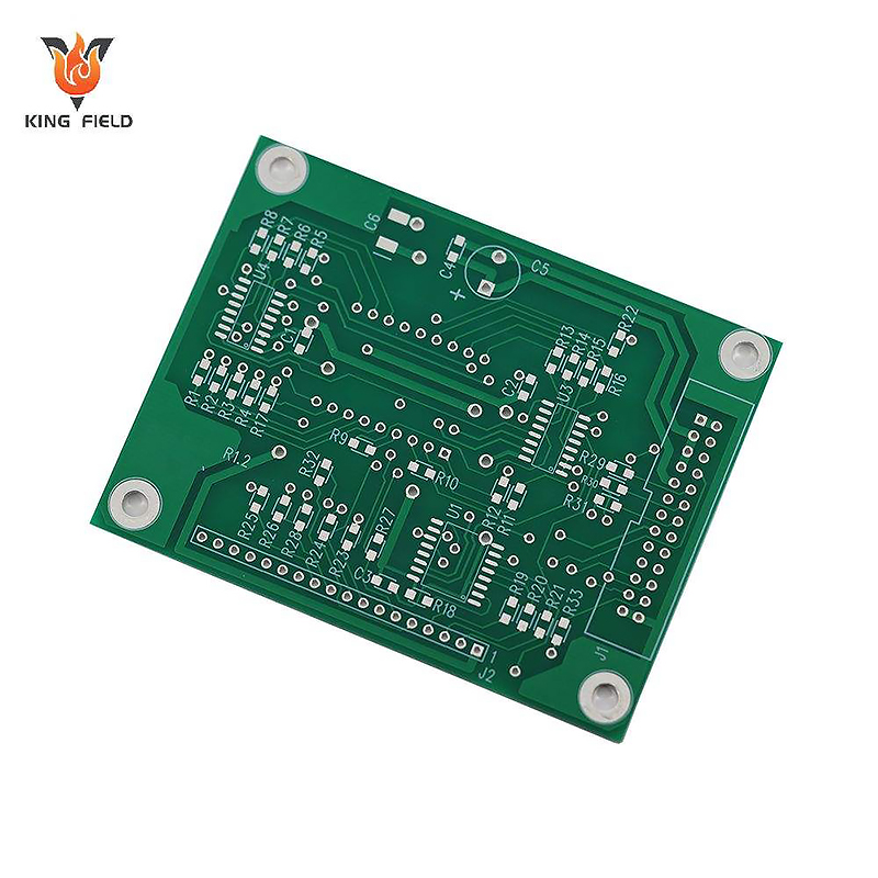
Substrate: FR4 KB
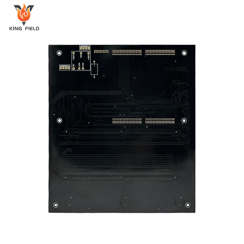
Shelves: 4 layers
Dielectric constant: 4.2
Plate thickness: 3.2MM
Outer copper foil thickness: 1 o z
Inner copper foil thickness: 1 o z
Surface treatment method: lead-free tin plating
FR4 PCB parameters
Project |
Parameter |
substrate |
FR4-KB |
Dielectric constant |
4.2 |
Plate thickness |
3.2MM |
Inner copper foil thickness |
1oz |
Minimum aperture |
0.3mm |
Minimum line spacing |
0.2MM |
number of floors |
4 floors |
use |
Industrial control |
Outer copper foil thickness |
1oz |
Surface treatment methods |
Lead-free tin plating , lead-free alloy |
Minimum line width |
0.2MM |
Substrate thickness |
0.1mm - 10.0mm |
Copper foil thickness |
1/3 oz - 3 oz |
Minimum line width/line spacing |
1/3 oz - 3 oz |
Minimum aperture |
0.2mm - 3.2mm |
Maximum board size |
600mm × 500mm |
number of floors |
Floors 1-20 |
Maximum operating temperature |
130°C (long-term), 150°C (short-term) |
Minimum BGA |
7 million |
Minimum SMT |
7*10mil |
Surface treatment |
ENIG, gold finger plating, immersion silver plating, immersion tin plating, HASL(LF), OSP, ENEPIG, flash gold plating; hard gold plating |
solder mask |
Green solder mask layer / Black PI layer / Yellow PI layer |
Conventional glass transition temperature |
130-140°C |
FR4 PCB board, choose KING FIELD for professional support
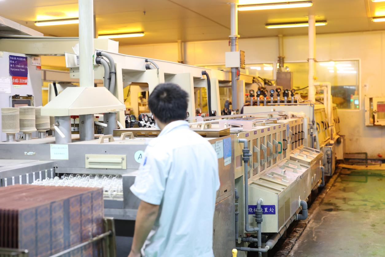
Our core team members all have over 20 years of PCB manufacturing experience . Since its establishment in 2017, KING... FIELD focuses on ODM, OEM, and PCB/ PCBA manufacturing , and is committed to providing customers with one-stop solutions from solution design to mass production delivery .
98.9% on-time delivery rate
Typically, the delivery time for KING FIELD's FR4 PCBs is 1-3 weeks, as detailed below:
• Expedited FR4 PCB service: 1-5 days;
• Prototyping and small-batch production: 1-2 weeks;
Mass production: 2-4 weeks.
Partners
KING FIELD's services cover the global market, providing all-inclusive and customer-supplied material FR4 PCB manufacturing services. We serve well-known clients such as PRETTL, Yadea, Xinri, and Schneider in Germany , and have gained recognition from many clients.
Full-cycle service guarantee
From initial design analysis to transparent production progress and rapid after-sales response , KING FIELD is committed to providing full-cycle technical services to reduce your project risks and ensure your products can be launched smoothly.
FAQ
Q1. How do you ensure that multilayer FR4 PCBs do not delaminate or bubble under harsh environments?
KING FIELD : We will use vacuum lamination to control temperature and pressure changes, fundamentally ensuring the strength and reliability of the lamination.
Q2. How do you ensure the reliability of PCB vias (VIAs) to prevent copper breakage or signal failure?
KING FIELD : We combine high-precision drilling with pulse electroplating technology, optimize various drilling parameters, and then use pulse electroplating to ensure that the copper layer in the hole is uniform .
Q3. How do you control linewidth accuracy and etching consistency?
KING FIELD : In the CAM stage , intelligent pre-compensation is performed on the graphic first . During production, LDI is used to avoid deformation, and then a fully automated etching line is used for precise control.
Q4. How do you prevent problems such as poor adhesion of solder mask (green oil), peeling, or bubbles ?
KING FIELD : We use a combination of chemical and mechanical cleaning for double cleaning, and then perform segmented pre-baking, strong exposure and full heat curing after printing to ensure that the solder mask has excellent adhesion, hardness and chemical resistance.
Q5. What methods do you use to ensure that the delivered circuit boards are flat?
KING FIELD : During the engineering design phase , our engineers provide advice on layer symmetry and support for material selection . In the production phase, we employ stress baking and strictly control the thermal processes at each stage. Finally , the finished products are flattened and packaged on pallets to ensure that the PCBs delivered to our customers are flat.