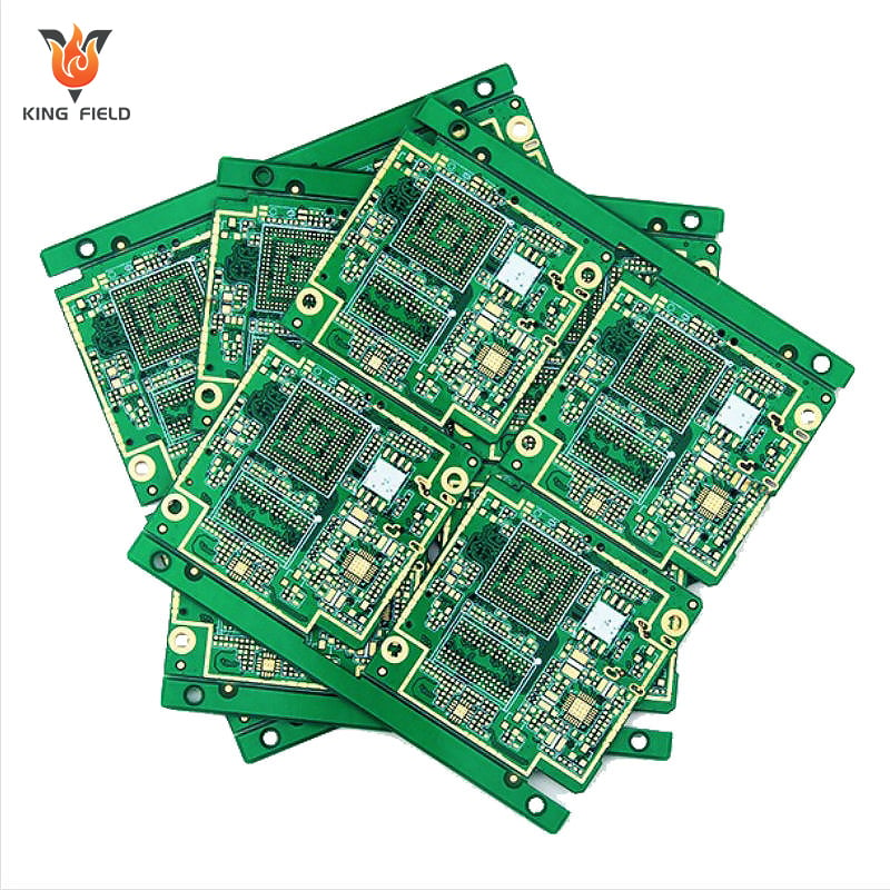
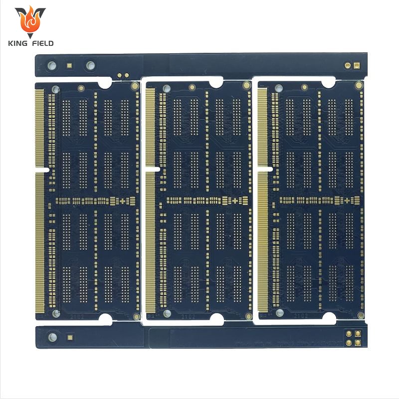
High-TG PCBs
With over 20 years of experience in PCB prototyping and manufacturing , KING FIELD prides itself on being your best business partner and close friend, and is dedicated to meeting all your PCB needs.
☑ Surface treatments : Electroless nickel-gold plating (ENIG), gold fingers, immersion silver, immersion tin, lead-free hot air leveling (HASL (LF)), organic solder mask (OSP), electroless nickel-palladium-gold plating (ENEPIG), flash gold, hard gold plating
☑ Sheet thickness range: 0.2mm-6.0mm
☑ Soldering process: Lead-free soldering compatible
Description
What is a high Tg printed circuit board?
High Tg A PCB is a printed circuit board manufactured using a special substrate designed to withstand higher operating temperatures. Therefore, high-Tg PCBs are sometimes referred to as high-temperature FR4 PCBs.
Material: Polyimide , FR4
Process: Sinking Gold
Minimum line width: 0.1mm
Minimum line spacing: 0.1mm
Number of floors: 2-40;
Sheet thickness range: 0.2mm-6.0mm;
Minimum line width/line spacing: 3mil/3mil;
Minimum aperture: 0.2mm;
Maximum board size: 610mm × 1220mm
Surface treatments: HASL, ENIG, OSP, etc.;
Soldering process: compatible with lead-free soldering;
Test standard: IPC-A-600 Level 2/3;
Certifications: UL, RoHS, ISO9001
Features: Single-ended differential impedance needs to be controlled precisely, trace width and spacing must be accurate, and BGA via plugging must not be spurious.
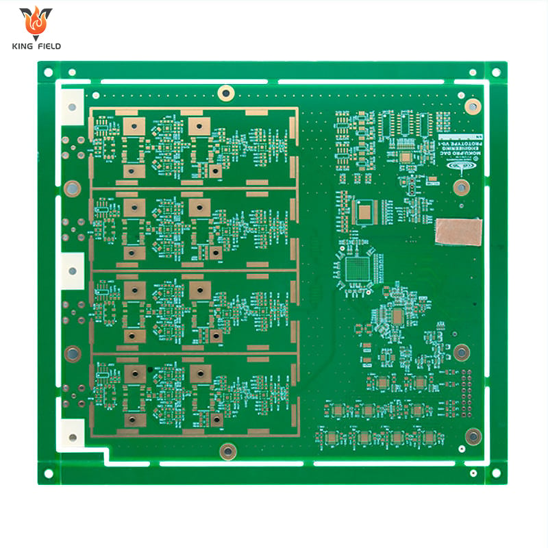
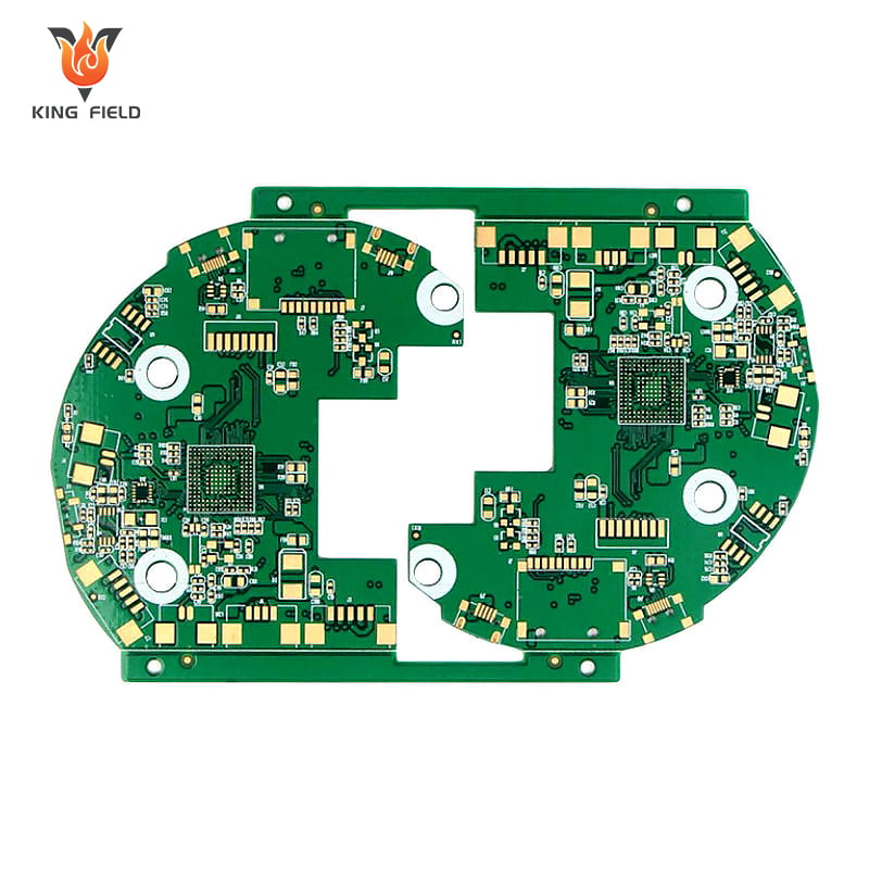
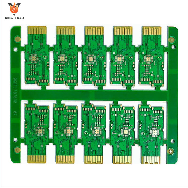
Main parameters of High-TG PCB
Substrate |
Polyimide , FR4 |
Dielectric constant: |
4.3 |
Outer copper foil thickness: |
1z |
Surface treatment method: |
Sinking Gold |
Minimum line width: |
0.1MM |
Application areas: |
Industrial control industry |
Shelves: |
Floors 2-60 |
Plate thickness: |
0.4-8 MM |
Inner copper foil thickness: |
1 |
Minimum aperture: |
0.2mm |
Inner layer minimum line width/spacing |
3/3 mil |
Minimum line width/spacing of outer layer |
3/3 mil |
Minimum board size |
10×10 MM |
Maximum board size |
22.5 x 30 inches |
Dimensional tolerances |
±0.1 MM |
Minimum Ball Grid Array (BGA) Pitch |
7. mil |
Minimum Surface Mount Technology (SMT) Pad Size |
7 × 10 mils |
Surface treatment |
Electroless nickel-gold plating (ENIG), gold fingers, immersion silver, immersion tin, lead-free hot air leveling (HASL (LF)), organic solder mask (OSP), electroless nickel-palladium-gold plating (ENEPIG), flash gold, hard gold plating |
Solder resist color |
Green, black, blue, red, matte green |
Minimum solder resist gap |
1.5 mil |
Minimum solder resist dam width |
3. mil |
silkscreen color |
White, black, red, yellow |
Minimum silkscreen width/height |
4/23 mil |
Minimum line spacing: |
0.1MM |
Features: |
Single-ended differential impedance needs to be controlled precisely, trace width and spacing must be precise, BGA via plugging must not result in false copper leakage, and warpage needs to be strictly controlled. |
Why is KING FIELD a reliable choice for your High TG PCB?
Since its establishment in 2017, KING FIELD has become a benchmark in the ODM/OEM PCB/PCBA manufacturing industry, leveraging over 20 years of manufacturing experience in the electronics sector.
We are committed to providing customers with one-stop solutions from solution design to mass production delivery, and with customer satisfaction as our ultimate goal, we have established long-term business partnerships with customers around the world.
Our products are widely used in consumer electronics, industrial, automation, automotive, agriculture, defense, aerospace, medical and security markets.
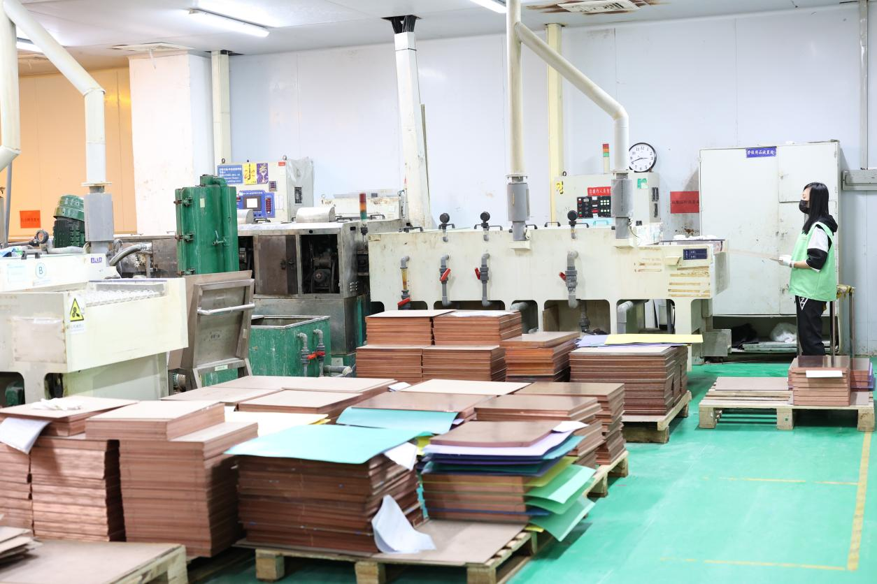
Our factory is equipped with a variety of assembly technologies, including SMT production and testing equipment, PTH insertion, COB, BGA, flip chip, wire bonding, assembly, and lead-free soldering.
We firmly believe that how we treat our employees, deliver our products, and solve problems will directly and powerfully influence our ability to exceed customer expectations.
20+ years of craftsmanship accumulation
High TG materials are far more difficult to process than ordinary FR4. However, our core team members have an average of 20+ years of practical experience in PCB/ PCBA, covering circuit design, process development, production management and other fields.
Comprehensive engineering support from product design to mass production
With KING FIELD offer one-stop electronic design and manufacturing facilities; from front-end R&D design, procurement of components, precision SMT placement, DIP insertion, complete assembly, and final functional testing - all happening at our PCB manufacturing platform.
Delivery capabilities verified by high-profile clients worldwide
Our High-TG PCBs have been regularly and continuously exported to markets in Europe, America, Japan, and South Korea, which is a testimony of our ability and dedication to conform to the highest international quality standards.
Transportation methods
Global Delivery : We regularly export to high-standard markets such as Europe, America, and Japan, and deliver the goods on time through air/sea freight with door-to-door services.
Working with reliable partners, we professionally ship internationally and, besides selling, we even support you through rapid response, full traceability, and we take complete responsibility for any issues after the delivery;

After-sales guarantee
KING FIELD is a 24-hour technical support service offering a pool of technical consultants to customer problems. We keep uninterrupted communication with the customers in the pre-sales consultation phase and follow-up response phase.
Being in close touch and coordination.
In this industry, we are one of the very few that provide "1-year warranty + lifetime technical consultation" services. If the product has a quality problem caused by non-human factors, we can provide free product returns and exchanges and cover the relevant logistics costs.
We also provide free PCB design optimization suggestions for customers' subsequent product iterations and technology upgrades. Our after-sales team's average response time is no more than 2 hours.
FAQ
Q1. How do you avoid rough hole walls or resin tearing?
KING FIELD : We use specialized high-hardness drill bits, and then precisely adjust the drilling speed and feed rate according to the specific TG value and structure of the plate material , laying the foundation for subsequent hole metallization and high-reliability electrical connection.
Q2. How do you ensure that the PCB will never delaminate or crack under high-temperature reflow soldering or long-term high-temperature operation?
KING FIELD : Before standard browning, we introduce plasma for cleaning , and then use a special high -temperature solution to create a stronger microstructure on the copper surface. Finally, we use computer- controlled vacuum pressing and precise curing parameters.
Q3. How do you prevent the solder mask (green oil) from blistering or peeling off during high-temperature soldering?
KING FIELD : We will use a special ink with a high crosslinking density that is matched with High TG boards, and then perform stepped temperature curing.
Q4. How do you ensure the alignment accuracy and dimensional stability of multilayer boards?
KING FIELD : We use a data-driven intelligent compensation system. First, we establish a database of the expansion and contraction of various High TG materials . During the engineering drawing stage , we perform differentiated compensation for each layer of the drawing.
Q5. How do you verify that the electrical performance of High TG PCB remains stable under high temperature conditions?
KING FIELD : Our R&D lab can perform full-temperature-range electrical performance verification, using a network analyzer to fully monitor changes in key electrical parameters from low to high temperatures.