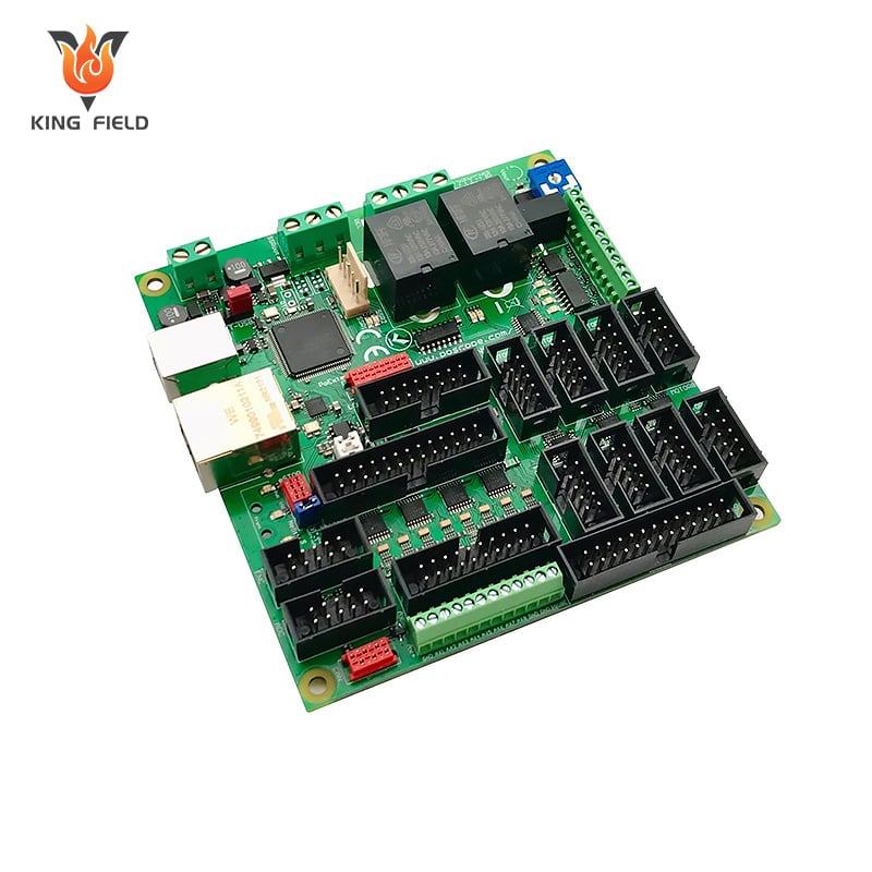
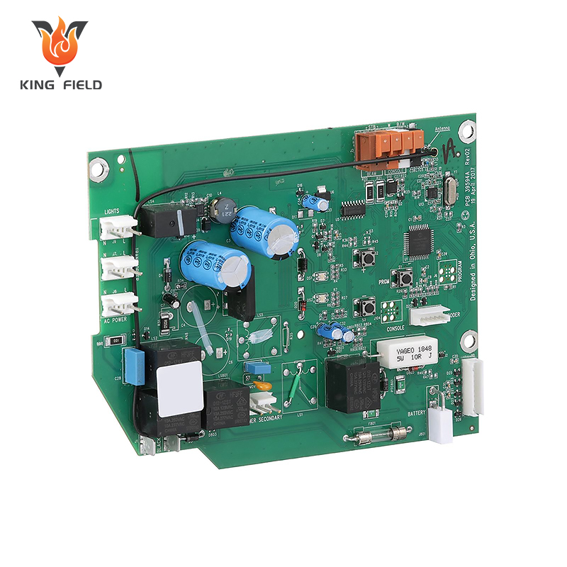
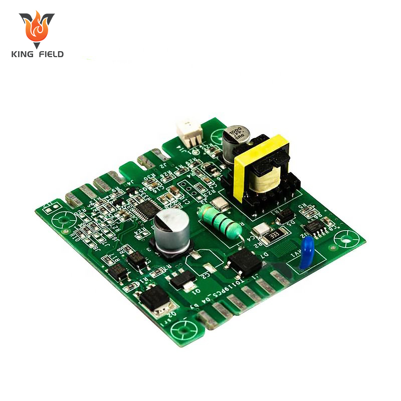
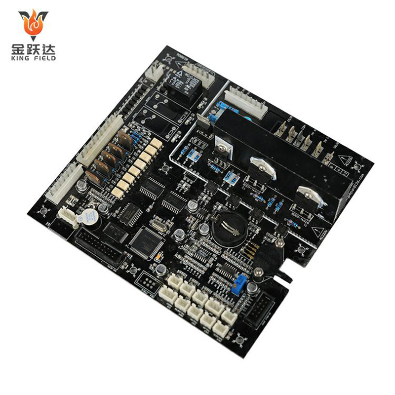
Medical PCBA
As a PCBA manufacturer with over 20 years of professional experience , KING FIELD is committed to providing high-quality, highly reliable Robot Assembly solutions to customers worldwide.
☑ Prototype samples: 24 hours to 7 days; Mass production: 10 days to 4 weeks
☑ Substrates : FR-4, high Tg FR-4, aluminum substrate, high frequency materials, flexible printed circuit board (FPC)
☑ Automated Optical Inspection (AOI), X-ray Inspection, Solder Paste Inspection (SPI)
Description
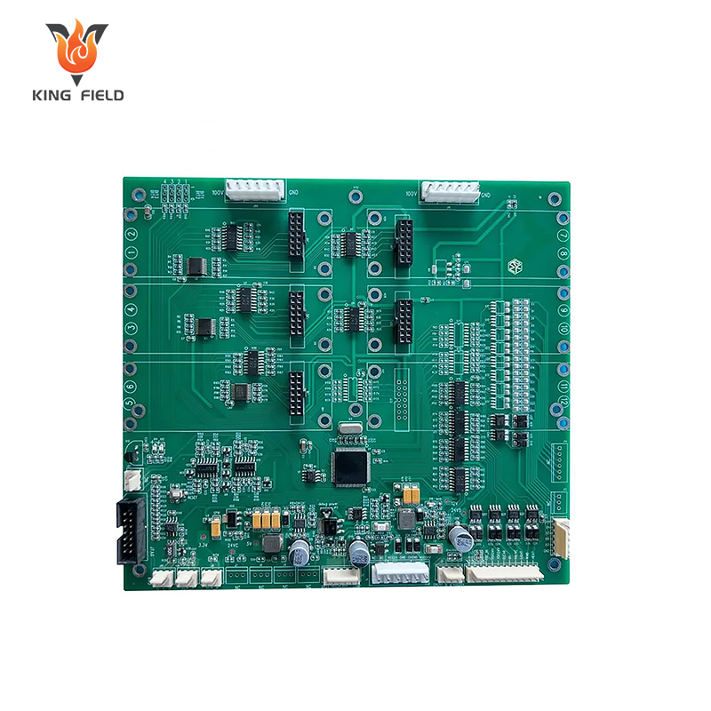
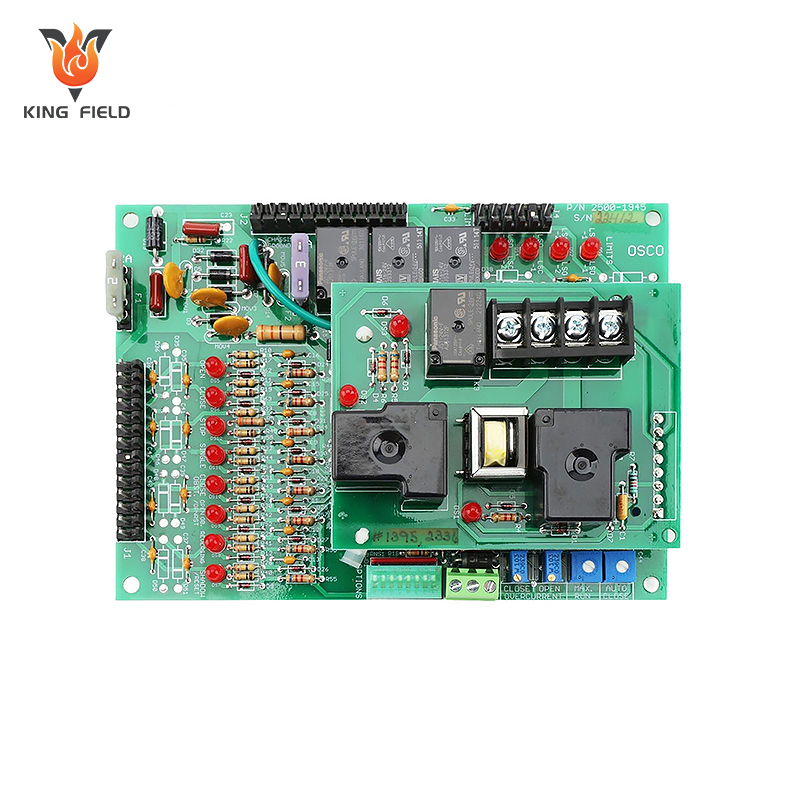
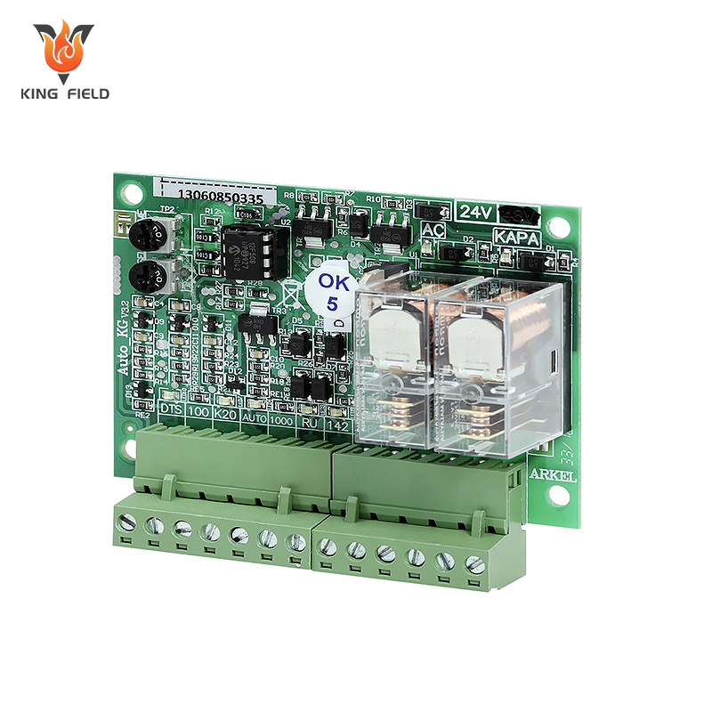
Materials: FR-4, high Tg FR-4, aluminum base, high frequency materials, flexible printed circuit board (FPC).
Product Features: Exact temperature control, timer function, several protections, first-class materials, and adjustable settings.
Technical advantages: Entire-cycle PCB assembly services, small runs of PCBA, OEM/ODM.
Surface treatments: Hot air solder leveling (HASL), chemical electroless gold plating, gold fingers, organic solder mask (OSP), chemical silver plating, electroless nickel-gold plating (ENIG), and electroless nickel-palladium-gold plating (ENEPIG).
Medical PCB assembly: A glance
Medical PCB assembly is the process of designing, manufacturing, and assembling printed circuit boards that are made for medical devices and equipment. The range of products in this industry is very varied, from simple diagnostic instruments to highly complicated life-support systems.
Project |
Parameter |
Board |
FR-4, high Tg FR-4, aluminum substrate, high frequency materials, flexible boards, rigid-flex boards, Rogers materials, biocompatible materials. |
Surface treatment |
Hot air leveling (HASL), chemical electroless gold plating, gold fingers, organic solder mask (OSP), chemical silver plating, electroless nickel-gold plating (ENIG), and electroless nickel-palladium-gold plating (ENEPIG). |
Impedance control |
up to ±10% or better accuracy |
solder paste type |
Lead-containing solder paste or lead-free solder paste |
Assembly process |
Reflow soldering, wave soldering, manual soldering, selective soldering |
Three-proof coating |
Acrylic acid, silicone, polyurethane, epoxy resin, parylene |
number of floors |
1-40+ floors |
Minimum line width |
0.10 mm (4 mils) |
Minimum line spacing |
0.10 mm (4 mils) |
Minimum aperture |
0.15 mm (6 mils) |
Detection method |
Automated Optical Inspection (AOI), X-ray Inspection, Visual Inspection, Solder Paste Inspection (SPI) |
Test methods |
In-Circuit Testing (ICT), Functional Testing (FCT), Flying Probe Testing, Boundary Scan Testing |
Medical-related certifications |
ISO 13485:2016 (Medical Device Quality Management System Certification) |
Quality certification |
ISO 9001:2015, IPC-A-600G Level II standard, IPC-6012B Level II standard, IPC-A-610 Level III standard |
Environmental compliance |
Compliant with RoHS, REACH, and UL 94V-0 standards. |
Delivery cycle |
Prototype samples: 24 hours to 7 days; Mass production: 10 days to 4 weeks |
Why is KING FIELD a reliable choice for your medical PCB assembly?
-
Deep accumulation
Founded in 2017, the core team of KING FIELD has been deeply involved in the PCBA field for more than 20 years, and we are dedicated to giving customers one-stop PCB/PCBA solutions.
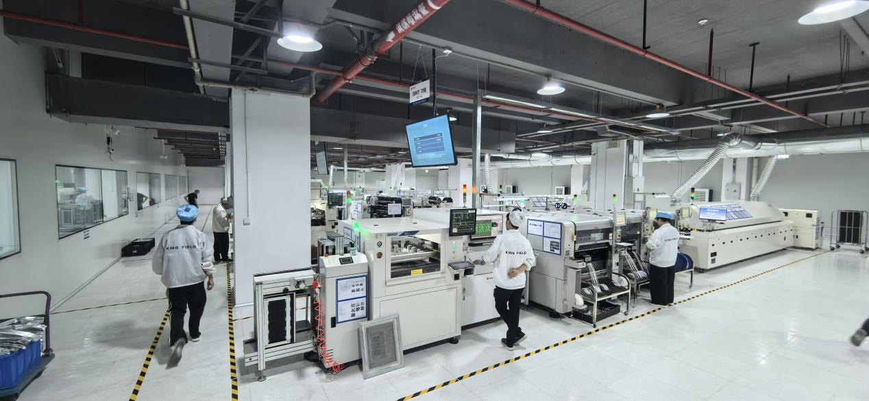
Our own plant
We have our own patch manufacturing plant, a Class 10,000 cleanroom, and dedicated medical production lines cover the factory area of more than 15,000 square meters.
Our production line consists of 7 SMT lines, 3 DIP lines, 2 assembly lines, and 1 painting line. Our YSM20R packs ±0.015mm placement accuracy and can mount the smallest 01005 components.We make 60 million SMT points and 1.5 million DIP points per day.
Export strength
Our products have been regularly exported to leading medical manufacturing countries such as Germany, the United States, Switzerland, and the United Kingdom, and deeply involved in:
High-end imaging equipment
Vital signs monitoring system
Portable diagnostic devices
KING FIELD guarantees that all products meet the medical electrical safety standards of the exporting country (e.g., IEC60601-1) and comply with RoHS/REACH environmental directives.
Testing and Verification of KING FIELD
It is of utmost importance to perform rigorous testing when dealing with medical PCB assembly. KING FIELD is known to rely on a range of tests, such as:
- In-Circuit Testing (ICT): Usually in-circuit testers are used to verify the only physical existence of components.
- Environmental testing:
- The changes such as temperature, moisture/vapor, mechanical vibration, etc.
- Checking the soldering quality via X-ray and visual/topical examination.
- Reliability testing (including HALT and HASS): The full forms of HALT and HASS are High Accelerated Life Testing and High Accelerated Stress Screening, respectively.
- Automated Optical Inspection (AOI)
- Solder joints that cannot be seen with the naked eye are inspected by X-ray.
- Online Testing (ICT)
- Functional testing
- Environmental stress screening
- Functional testing is basically a major method to verify that a device is really doing what it is supposed to do.

-
- Complimentary service
We promise to free of charge return or replace any product with a quality problem without human causation, and we will be responsible for the related logistics costs.
On average, the response time of our after-sales team is within 2 hours.
Usually, our problem-solving rate is up to 98%.
FAQ
Q1: What do you do to reduce particulate contamination during the assembly process?
We operate a Class 10,000 cleanroom, use medical-grade low-residue materials, and have an online cleaning system, plus we carry out ionic contamination and particulate testing for each batch.
Q2: How do you ensure reliable micro-pitch soldering in high-density medical boards?
We control micro-welding processes; micro-focus X-ray is used to monitor the void rate in BGA solder joints in real time; we also adopt structural reinforcements and perform accelerated life testing.
Q3: How do you eliminate the risk of electrolytic corrosion in medical devices during long-term usage?
We change material system, revamp process design, undertake corrosion simulation tests, elect pure tin or lead-free matte coatings to limit dendrite growth, and our conformal coatings meet IPC-CC-830B Class III certification.
Q4: How do you guarantee the biocompatibility of your implantable device PCBs over time?
We apply biocompatible certified materials, substrates have passed USP Class VI and ISO 10993-5 cytotoxicity tests, solders comply with ASTM F2066 implantable standards, and special processes like laser sealing and supercritical cleaning are used.
Q5: How do you satisfy the stringent traceability requirements for medical devices?
Our MES system is capable of carrying out full-process traceability for the manufacturing of every PCB/PCBA.