
 EN
EN
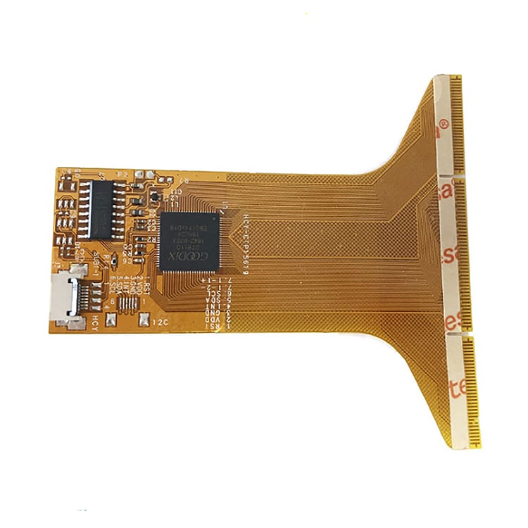
Space and Weight Optimization Through Flex PCB Manufacturing
The relentless miniaturization of portable electronics forces engineers to confront a fundamental physical limit: the rigid, planar geometry of traditional circuit boards consumes valuable three-dimensional space that is no longer available. Flex PCB manufacturing directly addresses this constraint by breaking the planar barrier—enabling circuits that fold, twist, and conform to the available envelope rather than dictating it. This design paradigm shift can reduce an assembly’s total footprint by 30–50% while simultaneously slashing weight—a dual advantage that is not merely incremental but transformative for device architecture.
Polyimide Substrates: Enabling Ultra-Thin, Lightweight, and Dimensionally Stable Designs
The foundational material advantage in flex PCB manufacturing is the polyimide film substrate, which replaces the woven glass-reinforced epoxy (FR-4) used in rigid boards. A standard rigid PCB layer with 1.6 mm thickness is an order of magnitude bulkier than a typical 0.125 mm polyimide core, and the weight differential is equally stark. Polyimide offers a density roughly 30% lower than FR-4 while providing superior thermal stability—with a glass transition temperature exceeding 250 °C—and a coefficient of thermal expansion that closely matches copper, minimizing stress during thermal cycling. This dimensional stability is critical for maintaining layer-to-layer registration in ultra-thin multilayer constructions. Its inherent flexibility is not a compromise but a deliberate property that allows the circuit to be folded into a 3D configuration during assembly, then held in a static bend, effectively occupying zero additional volume. Leading manufacturers now routinely produce 2-layer flex circuits with a finished thickness under 0.2 mm, enabling designers to fit complex interconnects into spaces previously reserved for thermal management or mechanical clearance.
3D Interconnectivity and Component Integration Eliminate Bulkier Cabling and Connectors
Beyond the material chemistry, the most dramatic space savings emerge from a system-level architectural change: replacing wire harnesses, ribbon cables, and board-to-board connectors with a single, formed flex circuit. In a conventional design, a connector pair can consume 5–10 mm of board height and require additional stiffeners and strain relief, whereas a flex-to-rigid transition adds virtually zero z-height. This consolidation eliminates not only the connectors themselves but also the labor, procurement, and potential failure points associated with each additional interconnect. A rigid-flex design can reduce total board area by 30–50% compared to a discrete rigid-board-plus-cable solution—a figure that translates directly into smaller, lighter end products. The ability to route a flex circuit’s arms around batteries, speakers, and sensors turns formerly dead volume into active interconnect space, a capability unavailable with any rigid alternative.
Mechanical Reliability: Flex PCB Manufacturing for Dynamic Bending and Harsh Environments
High Bend Cycle Endurance (>200,000 Cycles) Without Signal Loss or Delamination
Flex PCB manufacturing leverages polyimide substrates and rolled annealed copper to achieve exceptional dynamic bending longevity. By positioning conductors at the neutral bend axis—where tensile and compressive stresses cancel—designers minimize copper fatigue. Strain-relief structures and adhesiveless laminates further prevent delamination. According to IPC-2223 design guidelines, properly engineered flex circuits withstand over 200,000 bend cycles without signal degradation or layer separation. Laser-direct imaging creates precise, narrow traces that resist micro-cracking under repeated deformation. Controlled impedance is maintained even as the circuit flexes, ensuring consistent signal integrity. This endurance is essential for foldable hinges, wearable bands, and medical patches that undergo thousands of daily flex cycles. Long-term reliability tests confirm stable electrical performance after 200,000 cycles—making flex PCB manufacturing a critical enabler for motion-intensive applications where rigid boards would fail.
Robustness Against Shock, Vibration, and Thermal Cycling in Wearables and Portable Medical Devices
Wearable and point-of-care devices face sweat, mechanical shock, and wide temperature swings. Flex PCB manufacturing counteracts these stresses with polyimide’s inherent thermal stability and low mass—which naturally reduces vibration sensitivity. Conformal coatings and immersion silver finishes protect against humidity and corrosion. Under MIL-STD-202 thermal shock testing, circuits survived 1,000 cycles from −40°C to 125°C without delamination, confirming suitability for body-worn and outdoor use. Stiffeners at connector points prevent solder joint fatigue, while integrated antennas eliminate fragile wired connections. In hearing aids, continuous glucose monitors, and insulin pumps, such robust design ensures uninterrupted operation despite daily wear, accidental drops, and body heat. By combining material resilience with stress-optimized layouts, flex PCB manufacturing delivers the mechanical reliability required for portable medical electronics that must perform flawlessly in the most demanding environments.
Scalable Complexity: Multilayer and Rigid-Flex PCB Manufacturing in Sub-0.3mm Form Factors
Advancements in flex PCB manufacturing now extend multilayer and rigid-flex constructions into total thicknesses under 0.3 mm, delivering the scalable complexity essential for ultra-compact portables. By co-laminating rigid FR-4 and flexible polyimide layers in a single stack-up, rigid-flex designs eliminate bulky connectors and cabling, yielding profiles as slim as 0.25 mm in 4-layer configurations. Laser-drilled micro-vias (0.10 mm) and fine-line circuitry (0.04 mm) enable high-density routing without compromising mechanical integrity. The resulting assembly remains lightweight, withstands shock, vibration, and thermal cycling, and maintains a bend radius of just 24× the flex thickness—critical for wearables, implantable medical devices, and foldable smartphones. Manufacturing scalability is achieved through advanced materials and process controls that sustain yield even as layer counts rise to 12 or more, all while preserving the sub-0.3 mm form factor.
Real-World Applications Accelerating Flex PCB Manufacturing Adoption
Smartphones and Foldables: High-Density Interconnects for Cameras, Hinges, and Displays
Flex PCB manufacturing is the backbone of high-density interconnects in modern smartphones and foldables. Polyimide-based circuits enable the tight routing required for multi-lens camera modules, ensuring signal integrity without adding bulk. In foldable devices, dynamic flex circuits withstand hundreds of thousands of fold cycles across the hinge while maintaining reliable connections between halves. These ultra-thin assemblies also support edge-to-edge displays by allowing the driver IC to fold behind the screen, saving precious millimeters. As phone designs push for thinner profiles and seamless hinges, flex PCB manufacturing delivers the necessary combination of space efficiency, mechanical endurance, and robust long-term performance.
Wearables and Point-of-Care Devices: Conformal, Sweat-Resistant, and Antenna-Integrated Solutions
Flex PCB manufacturing supports the conformal, sweat-resistant, and antenna-integrated solutions required by wearables and point-of-care medical devices. Flexible circuits can be laminated into curved wristbands or skin patches, conforming to the body without compromising signal integrity. The use of biocompatible polyimide and thin copper layers enables reliable operation despite constant exposure to sweat and moisture. Integrated antenna patterns on the flex substrate eliminate separate rigid antennas, saving space and improving wireless connectivity. In point-of-care diagnostics, these circuits enable compact, disposable sensors that withstand repeated bending during patient use—driving faster adoption of portable health monitoring devices and improving patient compliance.
FAQ Section
What is flex PCB manufacturing?
Flex PCB manufacturing is the process of designing and producing flexible printed circuit boards made from polyimide substrates, which allow circuits to bend, fold, and conform to three-dimensional spaces.
Why is polyimide used in flex PCBs?
Polyimide is used because it is lightweight, ultra-thin, thermally stable, and dimensionally reliable, making it ideal for applications requiring flexibility and durability.
How do flex PCBs save space and weight?
Flex PCBs reduce the total footprint by 30–50% and eliminate bulky cabling and connectors, effectively shrinking device designs while maintaining or improving functionality.
What applications benefit most from flex PCB manufacturing?
Applications such as smartphones, foldable devices, wearables, and point-of-care medical devices benefit greatly due to their need for high-density interconnects, dynamic bending, and compact designs.
What is the reliability of flex PCBs in dynamic environments?
Flex PCBs are highly reliable in dynamic environments, capable of enduring over 200,000 bend cycles and functioning in harsh conditions such as thermal shock, vibration, and wear.
Table of Contents
- Space and Weight Optimization Through Flex PCB Manufacturing
- Mechanical Reliability: Flex PCB Manufacturing for Dynamic Bending and Harsh Environments
- Scalable Complexity: Multilayer and Rigid-Flex PCB Manufacturing in Sub-0.3mm Form Factors
- Real-World Applications Accelerating Flex PCB Manufacturing Adoption
- FAQ Section

