پیوندهای سریع
بردهای مدار چاپی (PCB) و مجموعههای بردهای مدار چاپی (PCBA) دو عنصر از مهمترین، اما رایجترین عناصرِ نادیدهگرفتهشده در طراحی و ساخت دستگاههای الکترونیکی مدرن هستند. اگر در حوزههای الکترونیک، سیستمهای تعبیهشده یا توسعه محصولات ابزاری فعالیت میکنید، درک تفاوت بین PCB و PCBA برای ساخت دستگاههایی قابلاطمینان، مقرونبهصرفه و پیشرفته ضروری است.
یک PCB ساختار اسکلتی است — یعنی تختهای بیجان و با دقت ساختهشده که ساختار فیزیکی و مسیرهای لازم برای اتصالات الکتریکی را فراهم میکند. خود PCB که از لایههایی از ماده اپوکسی تقویتشده با فیبرشیشه و مس هادی ساخته میشود، بدون اجزای الکترونیکی عملکردی ندارد. این مانند یک سیستم بزرگراه است که منتظر ترافیک است.
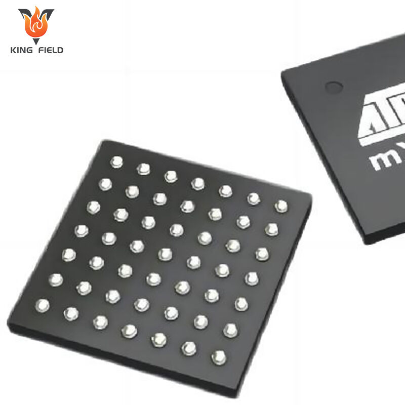
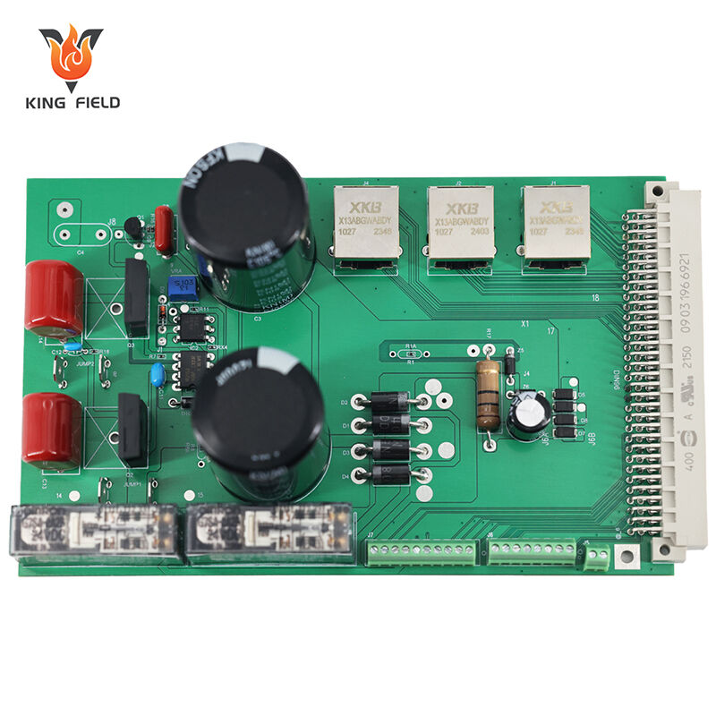
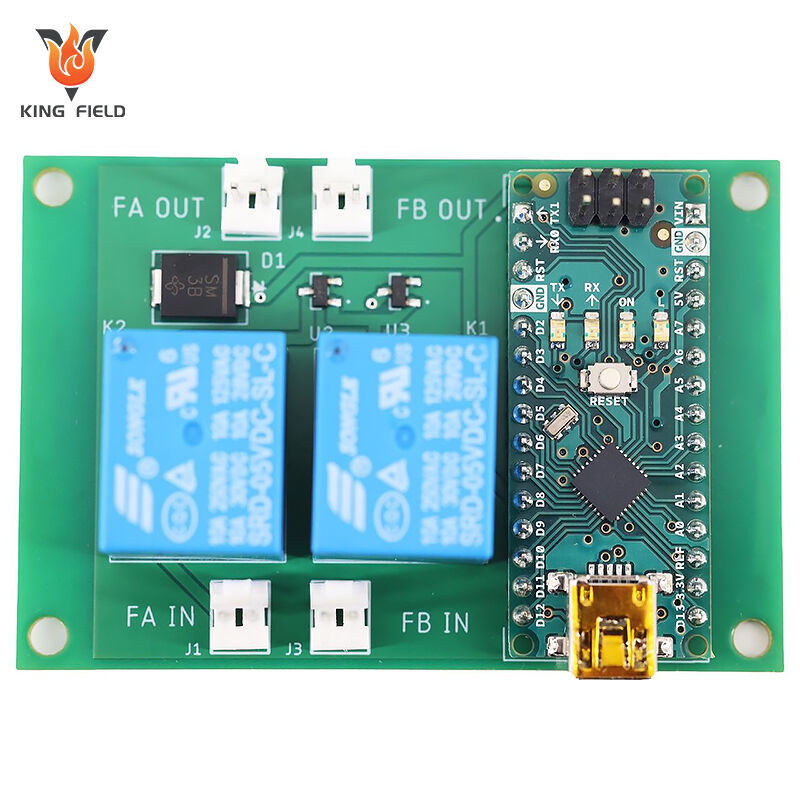
از سوی دیگر، PCBA (برد مدار چاپی مونتاژشده) نمایانگر مرحلهٔ بعدی توسعه است: این برد، مداری کامل، مونتاژشده و عملیاتی است. در اینجا، تمامی اجزای الکترونیکی غیرفعال و فعال — مانند مقاومتها، خازنها، دیودها و ادغامشدهها (ICها) — با دقت بالا بر روی برد مدار چاپی (PCB) توسط روشهای پیشرفتهای مانند فناوری نصب سطحی (SMT) یا فناوری سوراخگذاری از طریق بدنه (THT) لحیم میشوند. PCBA همان «مغز، اعصاب و اندامها» است که بر روی «اسکلت» (PCB) ساخته میشود و آن را به یک زیرسیستم الکترونیکی کاملاً عملیاتی تبدیل میکند.
برد مدار چاپی (PCB) سیستم اساسی تقریباً در هر دستگاه الکترونیکی امروزی است. اگر قبلاً یک رایانه، تلفن همراه، ریموت کنترل یا حتی یک مایکروویو را باز کردهاید، در واقع یک برد مدار چاپی را دیدهاید — معمولاً یک صفحهٔ سفت، تخت و سبزرنگ با ردیفهای مسی براق و حفرههای نصب، پورتها و علامتگذاریهای مختلف.
در هستهٔ خود، یک برد مدار چاپی (PCB) یک برد سیمکشی الکتریکی بدون عملکرد و بدون روکش است که از مواد محافظتی ساخته شده و لایههای نازک مس روی سطح آن لامینه شدهاند. این لایههای مس با دقت به خطوط رسانا تبدیل میشوند — همانند جادهها یا اتوبانها برای الکترونها — که با استفاده از دادههای طراحی و فرآیندهای تولیدی پیشرفته ایجاد میشوند. برخلاف روزگاران قدیمی که مدارها بهصورت دستی سیمکشی میشدند، بردهای مدار چاپی مدرن، توسعهٔ اتصالات الکتریکی را سادهتر و سیستماتیکتر میکنند.
کارایی و استحکام یک برد مدار چاپی (PCB) توسط کیفیت مواد اصلی و ساختار آن تعیین میشود. در ادامه، اجزای تشکیلدهندهٔ یک برد مدار چاپی مدرن آورده شده است:
|
بخش |
توضیحات |
هدف |
|
پایه |
معمولاً FR4، پلیایمید برای بردهای انعطافپذیر (flex PCB)، یا سایر گزینههای مختلف. |
استحکام مکانیکی و عایقبندی الکتریکی را فراهم میکند. |
|
لایههای مسی |
ورقههای نازک مس که روی زیرلایه لامینه شدهاند. |
سیگنالها و توان الکتریکی را هدایت میکند. |
|
ماسک لحیم |
لایهٔ محافظ، معمولاً پلیمر سبزرنگی که روی خطوط مسی قرار گرفته است. |
جلوگیری از اتصالات ناخواسته و سایش و فرسودگی، و تأمین رنگ. |
|
چاپ حریری |
لایهای نازک از چاپ سفید. |
برچسبها برای موقعیتیابی قطعات، شناسههای پیشنهادی و طرحهای لوگو. |
|
اتصالدهندههای جانبی |
پدهای تماس طلاآبکاریشده در امتداد لبه برد. |
اتصال برد مدار چاپی (PCB) به خروجیهای خارجی یا سیستمهای اتوبوس. |
|
Viaها |
سوراخهای فلزی ریزی که از طریق یک یا همه لایههای برد ایجاد شدهاند. |
اتصال الکتریکی لایههای مسی در جهتهای رو و زیر. |
پس از فرآیند دقیق طراحی و ساخت برد مدار چاپی (PCB)، برد حاصل همچنان تنها یک چارچوب بیجان است — «پردهای خالی» از مس، فیبرگلاس و تلاش. برای زندهکردن این پایه، وارد دنیای PCBA یا مونتاژ برد مدار چاپی میشویم. PCBA فرآیند ضروری است که برد مدار چاپی را به یک مغز دیجیتال زنده و پویا تبدیل میکند.
یک مجموعهی برد مدار چاپی (PCBA) برد مدار چاپی (PCB)ای است که تمام اجزای الکترونیکی آن — هم اجزای غیرفعال و هم اجزای فعال — بهدرستی روی آن قرار گرفته، متصل شده و لحیمکاری شدهاند. تنها پس از این مونتاژ، برد به یک مدار کاربردی تبدیل میشود که قادر به روشنشدن، پردازش اطلاعات و انجام وظایف عملی در دنیای واقعی است.
ویژگیهای کلیدی یک PCBA:
عملکرد بهعنوان مغز و اعصاب دستگاههای الکترونیکی
پردازش سیگنالها، اجرای منطق، ارتباطات و نظارت بر تغذیه
فراهمآوردن محیط فیزیکی و الکتریکیای که برای قابلیت اطمینان بهینهسازی شده است — و امکانپذیر کردن کاراییای را فراهم میکند که هم معیارهای بازار و هم انتظارات کاربر نهایی را برآورده میسازد
فرآیند ساخت یک PCBA شامل چندین مرحلهی دقیق و کنترلشده است:
اعمال خمیر لحیم: لایهای نازک از خمیر لحیم با استفاده از یک استنسیل روی پدهای اجزا چاپ میشود.
موقعیتیابی قطعات: ابزارهای پیکاندپلیس با سرعت بالا و کنترل کامپیوتری یا افراد متخصص، هر قطعه را در بهترین مکان آن بر اساس فایلهای طراحی PCB موجود در محل نصب میکنند.
لحیمکاری:
لحیمکاری با بازگشت حرارتی (Reflow soldering): برد در یک کوره بازگشت حرارتی قرار میگیرد که در آن دمای دقیقاً کنترلشده، لحیم را ذوب کرده و اتصالات مکانیکی و الکتریکی را ایجاد میکند.
لحیمکاری موجی (Wave soldering): بردها از روی موجی از لحیم مذاب عبور داده میشوند تا سرپایهها و پدها به یکدیگر متصل شوند.
تحلیل و کنترل کیفیت: روشهای پیشرفتهای مانند ارزیابی نوری خودکار (AOI)، ارزیابی با اشعه ایکس (برای BGAها) و ارزیابی بصری دستی، موقعیت قطعات، کیفیت سطح لحیم و شناسایی هرگونه عیب را تأیید میکنند.
آزمون عملیاتی: پس از نصب تمام قطعات، برد تحت آزمون مدار درونی (ICT) و آزمون مدار عملیاتی (FCT) قرار میگیرد تا عملکرد مناسب آن تأیید شود — که نشاندهنده تبدیل یک PCB خام به یک PCBA قابل اعتماد است.
بیایید بخشهای تشکیلدهنده یک PCBA کامل را بررسی کنیم. هر جنبه به قابلیت، قابلیت اطمینان و سهولت تولید آن اضافه میکند.
|
کامپوننت |
توضیحات |
نقش در PCBA |
|
Pcb خالی |
برد سفت یا انعطافپذیر با مس شکلگرفته |
چارچوب پایه و شبکه سیگنال |
|
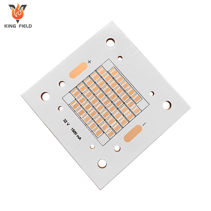
اجزای ساده |
مقاومتها، خازنها، سیمپیچها |
مدیریت جریان، ولتاژ و سیستم فیلتراسیون |
|
مولفههای فعال |
مدارهای مجتمع (IC)، میکروکنترلرها، دیودها، ترانزیستورها |
امکان پردازش، منطق، حسگری و تقویت را فراهم میکنند |
|
اتصالات |
پورتهای USB، آداپتورهای جانبی، سوکتهای سری، سوکتها |
اجازه دادن به رابطهای برقی خارجی |
|
لایهگذاری و شیمیایی فلزکاری (سولدر و فلوکس) |
پاست سولدر، میلهها و رشتهها؛ عامل تغییردهنده |
اتصال اجزا از نظر مکانیکی و الکتریکی |
|
پوششهای سطحی |
ENIG، HASL، OSP، نقرهآبی/قلعآبی غوطهور |
محافظت از مس و ایجاد نقاط لحیمکاری قابل اعتماد |
|
چسبها |
چسبهای اپوکسی و UV-curing |
ثابتکردن اجزای بزرگ یا حساس به ارتعاش |
کارایی: با نصب حرفهای اجزای برجسته و تضمین اتصالات لحیمکاری قابل اعتماد، مونتاژ برد مدار چاپی (PCBA) به اهداف کارایی مورد نیاز در کاربردهای امروزی — از دستگاههای هوشمند و خودروهای الکتریکی (EV) تا اسکنرهای MRI و ماهوارهها — دست مییابد.
یکپارچگی: تولیدکنندگان PCBA کنترلهای کیفیت سختگیرانهای اعمال میکنند— از جمله تحلیل، آزمونها و رعایت استانداردهایی مانند IPC-A-610 و ISO 9001— تا از موفقیت محصول حتی در شرایط سخت یا حیاتی از نظر ایمنی اطمینان حاصل شود.
مقیاسپذیری: روشهای خودکار مونتاژ از تولید انبوه دستگاههایی با حجم بسیار پایین تا صدها هزار دستگاه تولید انبوه پشتیبانی میکنند.
مسیر تبدیل یک برد مدار چاپی خام (PCB) به یک برد مدار چاپی مونتاژشده (PCBA) توسط فرآیند مونتاژ انتخابشده تعیین میشود. مناسبترین روش، قابلیت اطمینان، هزینه، کوچکسازی و همچنین بازار کاربردی محصول شما را شکل میدهد. هر روش به نیازهای خاص طراحی مدار پاسخ میدهد— از جمله حفظ پهنای باند بالا، توان، مقاومت مکانیکی و همچنین نیازهای حجمی.
توسعه سطحی (SMT) رویکرد غالب برای نصب بوردهای امروزی کوچک و پرقدرت است. SMT با امکانپذیر کردن طراحیهای مداری بسیار متراکم و اتوماسیون پیشرفته، الکترونیک را دوباره اختراع کرده است.
نوع قطعه: قطعات نصبشده روی سطح (SMDها)، که دارای ترمینالهای فلزی کوچکی هستند، مستقیماً روی پدهای مسی قرار میگیرند.
فرآیند مونتاژ:
چاپ از طریق استنسیل: استفاده از خمیر لحیم با الگوی دقیق روی پدهای مشخص.
برداشتن و قرار دادن: ماشینآلات اتوماتیک بهسرعت SMDها را با استفاده از اطلاعات موجود در اسناد مرکز جرم (Centroid) روی پدهای پوشیدهشده با خمیر لحیم قرار میدهند.
لحیمکاری با بازگشت حرارتی (Reflow): برد وارد کورهای کنترلشده میشود؛ خمیر لحیم ذوب شده و قطعات را محکم میبندد.
ارزیابی نوری اتوماتیک (AOI): دوربینها به دنبال جابجاییهای نادرست، اتصال کوتاه، قطعات از قلمافتاده یا وارونهشده و عیوب لحیمکاری میگردند.
تحلیل با اشعه ایکس: برای BGAها و دستگاههایی با اتصالات پنهان، تصویربرداری اشعه ایکس اطمینان از ایجاد اتصالات محکم را فراهم میکند.
کوچکسازی جدی.
نصب با سرعت بالا و حجم بالا.
قابلیت نصب اجزای دوطرفه.
افزایش عملکرد الکتریکی در نتیجه کاهش ابعاد مسیرهای مدار و اندوکتانس.
کاربردهای معمول SMT:
ابزارهای دیجیتال مصرفکننده.
تجهیزات با سرعت بالا.
الکترونیک پزشکی و خودرو که ضخامت در آنها حیاتی است.
فناوری نوین سوراخدار (THT) اولین روش مونتاژ است و همچنان برای کاربردهایی که به مقاومت مکانیکی و دوام بهینه نیاز دارند، اهمیت زیادی دارد.
نوع المان: پایهها (پایههای فلزی) از طریق سوراخهای ایجادشده در برد مدار چاپی (PCB) عبور میکنند.
تنظیم مرحله بهینهسازی (Refine):
نصب قطعات: المانها بهصورت دستی یا با ابزارهای نیمهخودکار دقیقاً در سوراخهای متناظر روی برد قرار داده میشوند.
لحیمکاری موجی (Wave Soldering): برد از روی «موج»ی از لحیم مذاب عبور میکند که از طریق سوراخها بالا آمده و پایهها و مساحتهای لحیمکاری را به هم متصل میکند.
برش اضافهپایهها و پاکسازی: پایههای اضافی برش داده میشوند؛ باقیماندههای فلاکس پاک میشوند.
ارتباطات مکانیکی قویتر؛ مناسب برای قطعات بزرگ یا سنگین.
قابلیت اطمینان بالاتر در محیطهای با ارتعاش شدید یا شرایط سخت.
برای بازبینی و تعمیر دستی، ساخت نمونه اولیه (پروتوتایپ) و راهاندازی حجم پایین و سفارشی، انجام آسانتری دارد.
کاربردهای معمولی THT:
هوا-فضا، نظامی و الکترونیک خودرو.
دستگاههای الکترونیک قدرت، ترانسفورماتورها، پورتها و رلهها.
کنترلهای صنعتی که بر اساس شرایط شدید ضربه، رزونانس و دما طراحی شدهاند.
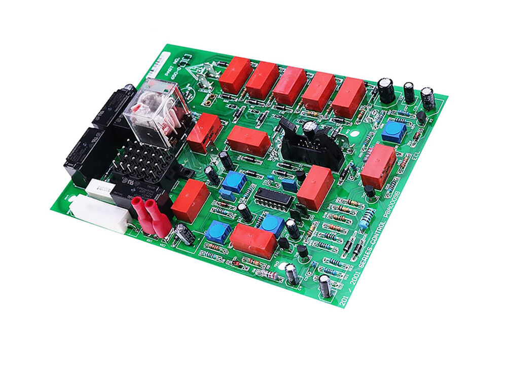
مونتاژ ترکیبی از هر دو روش SMT و THT استفاده میکند و از نقاط قوت هر یک از این روشها بهره میبرد.
مدارهای چاپی (PCB) صنعتی اغلب نیازمند SMT برای مدارهای دیجیتالی/ارتباطی با تراکم بالا و THT برای اتصالدهندههای با دوام، ترانسفورماتورها یا اجزایی هستند که گرما را پخش میکنند.
امکان ترکیب انعطافپذیر را فراهم میکند؛ مثلاً کنترلکننده پهپاد ممکن است از تراشهها و سنسورهای SMT و همچنین از اجزای THT برای دریچههای ورودی برق و خازنهای بزرگ استفاده کند.
عناصر SMT ابتدا ایجاد و لحیمکاری میشوند (لحیمکاری با بازگشت حرارتی).
عناصر THT نیازمند قرارگیری و لحیمکاری با موج هستند.
بردهای نهایی ممکن است از بازرسی ترکیبی و آزمونهای چندمرحلهای عبور کنند.
اگرچه اصطلاحات PCB و PCBA گاهی بهصورت متقابل استفاده میشوند، اما در واقع نمایانگر مراحل متمایزی در فرآیند ساخت دستگاههای الکترونیکی هستند؛ هر کدام ویژگیها، هزینهها، الزامات فنی و کاربردهای بازار خاص خود را دارند.
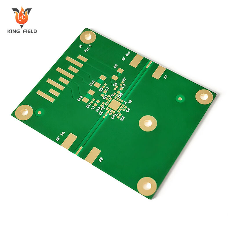
PCB (برد مدار چاپی): PCB یک برد سازمانیافته و غیرفعال است — یک برد سیمکشی خالی که از لایههای زیرلایه (مانند FR4)، مسارات مسی، ماسک لحیم و سیلکاسکرین تشکیل شده است. عملکرد آن ارائه حمایت مکانیکی و مسیرهای الکتریکی برای قطعات آینده است، نه اینکه بهتنهایی بهعنوان یک مدار عمل کند.
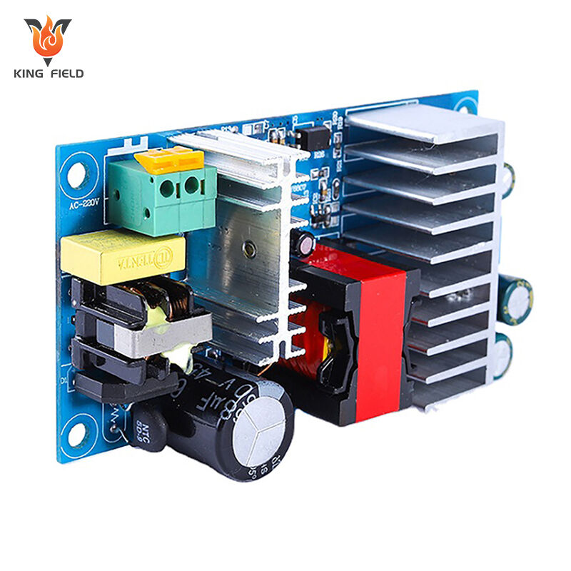
PCBA (مونتاژ برد مدار چاپی): PCBA برد کاملشده است — به عبارتی، برد مدار چاپی (PCB) که تمام قطعات الکترونیکی مورد نیاز (غیرفعال و فعال) روی آن قرار گرفته و لحیمکاری شدهاند. در حال حاضر این برد یک ماژول الکترونیکی عملیاتی است که محاسبات، کنترل، تعامل، نظارت بر توان یا تشخیص را انجام میدهد.
نکات تولید PCB:
قالببندی: طراحی CAD، تولید اسناد Gerber.
تولید: آمادهسازی زیرلایه، لایهنشانی مس، اچ کردن الگو، سوراخکاری، پوششدهی، ماسک لحیم، چاپ سیلکاسکرین، پایانهسازی سطحی و بازرسی نهایی.
نکات تولید PCBA:
آمادهسازی نصب: فهرست قطعات (BOM)، دادههای انتخاب و قراردادن (Pick-and-Place) و مرکز جرم (Centroid)، تأمین قطعات.
نصب قطعات: فناوری نصب سطحی (SMT) و/یا فناوری نصب از طریق سوراخ (THT).
لحیمکاری: لحیمکاری با بازگشت حرارتی (Reflow) برای SMT و لحیمکاری موجی (Wave Soldering) برای THT.
ارزیابی و آزمون: بازرسی بصری خودکار (AOI)، تصویربرداری با اشعه ایکس (X-ray)، آزمون مدار درجا (ICT)، آزمون عملکردی (FCT) و بررسیهای کاربردی.
|
جنبه |
PCB |
PCBA |
|
عملکرد |
پایه بیحرکت |
مدار الکترونیکی کاملاً کاربردی. |
|
تمرکز طراحی |
ردیابی انتقال سیگنال، تراشهبندی لایهها، طراحی برای ساخت (DFM) |
سبک قطعات، استراتژی لحیمکاری، غربالگری |
|
سفارشیسازی |
مatters لایهها، مواد، پوشش نهایی |
انتخاب قطعات، فرمافزار رومیزی (firmware)، راهاندازی سریها |
|
بررسی نیازها |
آزمون الکتریکی (E-test)، پیوستگی، اتصال کوتاه |
آزمون در مدار، آزمون عملکردی، آزمون محیطی، بازرسی اپتیکی خودکار (AOI)، رادیوگرافی اشعه ایکس (X-ray) |
|
قابلیت بازکاری |
برخی (ردپای برش/پرش) |
تسهیلات (نیازمند لحیمکندن است که ممکن است پدها را آسیب دهد) |
برد مدار چاپی (PCB): هزینهای از کم تا متوسط به ازای هر واحد؛ عمدتاً توسط ابعاد برد، تعداد لایهها، نوع محصول و روکش تعیین میشود. مناسب برای خودکارسازی و ساخت نمونه اولیه.
برد مدار چاپی مونتاژشده (PCBA): نرخ سیستمی بالاتر؛ شامل هزینههای زیر میشود:
خرید قطعات.
نیروی کار یا خودکارسازی مونتاژ.
نظارت و کنترل کیفیت.
تلفات ناشی از مشکلات راهاندازی.
روالهای شامل تمیزکاری، ارزیابی و بستهبندی محصول.
برد مدار چاپی (PCB): سریعترین زمان انجام — تنها ۲۴ تا ۷۲ ساعت برای نسخههای سریعالاجرا یا ۱ تا ۲ هفته برای تولیدهای سنتی، بسته به پیچیدگی طراحی.
برد مدار چاپی مونتاژشده (PCBA): زمان انجام طولانیتر، معمولاً ۲ تا ۴ هفته یا بیشتر، به دلیل وابستگی به زنجیره تأمین قطعات، برنامهریزی مونتاژ و تست پس از مونتاژ.
برد مدار چاپی (PCB): بهصورت تختههای خالی تحویل داده میشود؛ توسط مهندسان برای ساخت نمونه اولیه یا در شرکتهایی با خط تولید اختصاصی خود استفاده میشود.
بستهبندی: خلاءبسته، قابل انباشتهشدن، مقاوم در برابر رطوبت.
برد مدار چاپی مونتاژشده (PCBA): بهصورت قطعات کامل و آمادهٔ ادغام تحویل داده میشود؛ در تولید نهایی استفاده میشود و آمادهٔ ادغام در محیط یا سیستم است.
بستهبندی: با تقسیمبندی داخلی، ضد الکتریسیتهٔ ساکن، و معمولاً با جعبههای سفارشیشده برای محافظت از قطعات حساس.
بردهای مدار چاپی (PCB) زمانی انتخاب میشوند که:
در ابتدای چرخه حیات محصول (ساخت نمونه اولیه، تحقیق و توسعه).
شرکتها تمایل دارند خود را ایجاد یا تغییر دهند.
کاهش هزینههای اولیه تولید ضروری است.
PCBAها زمانی ترجیح داده میشوند که:
گزینههای کامل ترجیح داده میشوند (پیچیدگی را بهصورت قراردادی برونسپاری کنید).
زمان کوتاه برای عرضه محصول در بازار حیاتی است.
امکانات، مدارهای با کیفیت بالا یا سرعت بالا مورد نیاز است.
تواناییها یا ابزارآلات لازم برای راهاندازی وجود ندارند.
بردهای مدار چاپی (PCB) و مجموعههای بردهای مدار چاپی (PCBA) مراحل متوالی و همکارانهای در فرآیند ساخت ابزارهای الکترونیکی را نشان میدهند — رابطهای همکارانه که در قلب هر محصول دیجیتال هوشمند قرار دارد.
یک PCB نقطه آغازین برای هر نوع دستگاه الکترونیکی مدرن است. این مدار عملکردهای زیر را ایفا میکند:
اسکلت مکانیکی — که چیدمان و موقعیت اجزا را تعیین میکند.
شبکه اتصالدهنده — که مسیرهای الکتریکی برای سیگنالها و تغذیه را تعریف میکند.
«پارچه طراحی» — جایی که تمامی فرآیندهای خط تولید در آینده، قطعات را روی آن قرار داده، لحیم کرده و آزمایش میکنند.
یک PCBA زمانی ایجاد میشود که PCB خالی با تمامی اجزای الکترونیکی مورد نیازش، با استفاده از روشهای نصب سطحی (SMT)، نصب از طریق سوراخ (THT) یا روشهای ترکیبی تجهیز شود.
وابستگیهای کلیدی:
ساخت PCBA بدون وجود PCB امکانپذیر نیست: زیرلایه، ردیفهای مسی، ویاها و صفحات لحیمکاری روی PCB، حمایتهای ضروری برای هر یک از اجزای الکترونیکی در طول فرآیند تجهیز هستند.
دقت، تمیزی و کیفیت مادی PCB بهطور مستقیم بر قابلیت لحیمکاری، صحت الکتریکی و قابلیت اطمینان بلندمدت PCBA تأثیر میگذارد.
تمرکز: توالی لایهها، صحت سیگنال، مقاومت مکانیکی.
نتیجه: برد خالی غیرعملیاتی اما قابل آزمون.
تأکید: انتخاب قطعات، قرارگیری دقیق، لحیمکاری پایدار و آزمونهای گسترده.
نتیجه نهایی: مدار عملیاتی — آماده ادغام در محصول نهایی.
برد مدار چاپی (PCB): معمولاً در خلاء بستهبندی شده، بارگذاری و طبقهبندی میشود — خطر بسیار کم و حملونقل بسیار آسان.
برد مدار چاپی مونتاژشده (PCBA): نیازمند بستهبندی شخصیسازیشده ضد الکتریسیته ساکن (ESD)، با جداسازی اجزا در بخشهای مجزا برای محافظت از اجزاء حساس و اتصالات لحیمی ظریف در برابر الکتریسیته ساکن، دستزدن و ارتعاش.
ساخت برد مدار چاپی (PCB) معمولاً پایه ماژولار در زنجیره تأمین است و امکان انعطافپذیری بالا را فراهم میکند: طراحیها و مشخصات مختلف PCB برای محصولات متنوع یا نیازهای خاص مشتریان.
تاسیس PCBA جایی است که اقلام از هم جدا میشوند، بازرسی میشوند و ارزش افزوده به آنها اعمال میگردد — و این امر از ساخت سریع نمونههای اولیه تا ارائه راهحلهای نهایی برای تولیدکنندگان تجهیزات اصلی (OEM) در بازار انبوه پشتیبانی میکند.
بردهای مدار چاپی (PCB) و مجموعههای بردهای مدار چاپی (PCBA) ساختار فیزیکی و ارزشمند عصر دستگاههای دیجیتال را ایجاد میکنند. سادگی، مقیاسپذیری و قابلیت سفارشیسازی آنها امکان دستیابی به نوآوریهای بیسابقه را در حوزههای مختلف فناوری فراهم کرده است. چه به شکل یک برد تکرویه ساده و چه به صورت یک برد چندلایه با تراکم بالا و کاملاً پر شده، این اساسها در تقریباً تمامی صنایع امروزی حیاتی شدهاند.
PCBها و PCBAها در قلب ابزارهای مصرفکننده مدرن قرار دارند — جایی که تراکم، کارایی هزینهای و عملکرد بالا ضروری هستند.
مزایای رایج PCBA:
تلفنهای هوشمند و تبلتها: PCBAهای چندلایه، توان، پردازش، سنسورها، ارتباطات و آنتنها را در فضاهای فوقالعاده نازک مدیریت میکنند.
لپتاپها و رایانههای خانگی: مادربردهای پیچیده با قطعات SMT و THT بهصورت متراکم و فشرده، که از پردازندههای سریع، حافظه و ورودی/خروجی پشتیبانی میکنند.
دستگاههای قابل پوشیدن: PCBهای/PCBAهای فوقالعاده کوچک و انعطافپذیر که بهطور اختصاصی برای افزایش بهرهوری، طول عمر باتری و ارتباط بیسیم طراحی شدهاند.
لوازم خانگی و سرگرمی: بردهای دوطرفه یا چندلایه که مدارهای کنترلی تلویزیونها، ماشینهای لباسشویی، دستگاههای سرمایشی، بلندگوهای هوشمند صوتی و بسیاری از دستگاههای دیگر را اجرا میکنند.
روند جهانی سمت الکتریکیشدن، خودکارسازی و اتصال در کامیونها، به راهحلهای قوی و قابل اعتماد PCB/PCBA وابسته است.
کاربردهای محرمانه شامل:
واحدهای کنترل موتور (ECU) / کنترل گیربکس: PCBهای/PCBAهای چندلایه با الزامات سختگیرانه در زمینه دما، ارتعاش و تداخل الکترومغناطیسی (EMI).
مدیریت باتری در خودروهای الکتریکی (EVها): PCBهای/PCBAهای مسی با ضخامت بالا برای مدیریت جریان و ایمنی و حفاظت.
سیستمهای پیشرفته کمک به رانندگی (ADAS): تنظیمات چندلایه با سرعت بالا و بهینهشده برای فرکانسهای رادیویی (RF)، مناسب برای رادارها، دوربینهای دیجیتال و ترکیب سیستمهای تشخیص.
تبلیغات تلویزیونی و ناوبری: بردهای پیچیده با امکانات HDMI، GPS، بلوتوث و رابط کاربری پیشرفته.
سیستمهای اتوماسیون صنعتی، رباتیک و کنترل، به PCBهایی نیاز دارند که مقاوم، قابل اعتماد و برای محیطهای سخت طراحی شدهاند.
امنیت و دقت در مراقبتهای بهداشتی و درمانی از اهمیت بالایی برخوردارند؛ بنابراین PCBها باید بالاترین الزامات را از نظر یکپارچگی و زیستسازگاری برآورده کنند.
دستگاههای رایانشی کارآمد متکی به PCBهای چندلایه و پرسرعت هستند تا اتصالات متراکم برای پردازش، حافظه و توزیع توان را پشتیبانی کنند.
زیرساختهای مخابراتی به PCBهایی وابستهاند که قادر به تحمل فرکانسهای بالا، تلفات کم و عملکرد حرارتی ایمن و پایدار باشند.
شرایط معمول استفاده:
ایستگاههای پایه، سوئیچها و روترها: بردهای چندلایه بهینهشده برای فرکانس رادیویی که امکان تعاملی سریعالسیر و بدون خطا را فراهم میکنند.
قطعات بیسیم: واحدهای چاپی مدار مجتمع (PCBA) فشرده و امن برای عناصر ۵G/LTE، وایفای و بلوتوث.
در فناوریهای هوافضا، نظامی و ماهوارهای، بردهای چاپی (PCB) و واحدهای چاپی مدار مجتمع (PCBA) در معرض سختترین شرایط عملیاتی جهان قرار میگیرند.
کاربردهای پیشرو:
سیستمهای کابین و الکترونیک هوانوردی: بردهای انعطافپذیر-صلب و مقاوم در برابر تابش برای حفظ تمامیت کامل و کاهش وزن.
سیستمهای ماهوارهای: واحدهای چاپی مدار مجتمع (PCBA) سبکوزن، مقاوم در برابر تغییرات دما و تأییدشده در برابر لرزش برای پردازش سیگنال و تلهمتری.
سیستمهای راهنمایی، موشکی و راداری: مونتاژهای فوقالعاده مقاوم با مسیرهای مسی تکراری و محافظتشده و روشهای پیشرفته تست و غربالگری.
کوچکسازی، بهرهوری انرژی و طول عمر بالا، روند طراحی بردهای چاپی (PCB) و واحدهای چاپی مدار مجتمع (PCBA) در دستگاههای اینترنت اشیا را تعیین میکنند.
کاربردهای برجسته:
دستگاههای جمعآوری از راه دور و برچسبهای هوشمند: مدارهای چاپی (PCBA) کوچک، با مصرف انرژی بسیار پایین و قابلیت استفادهی گسترده برای مکانیابی دقیق و مصرف باتری بسیار کم.
اجزای خانه هوشمند: مدارهای چاپی تکرو یا دورو برای دکمهها، دستگاههای تشخیص محیط و کنترلکنندهها.
اینترنت اشیاء صنعتی (IIoT): مدارهای چاپی مقاومسازیشده برای جمعآوری دادهها و کنترل در محل نصب.
انتخاب بین ساخت مدار چاپی بدون مونتاژ (Bare PCB) و راهحل کامل مونتاژشده (PCBA) تصمیمی حیاتی در چرخه عمر محصولات الکترونیکی است. این انتخاب بر هزینهها، زمانبندیها، نیازهای ارزیابی، پیچیدگی زنجیره تأمین و در نهایت موفقیت پروژه شما تأثیر میگذارد. بهترین انتخاب به منابع فنی، مقیاس تولید، زمانبندی و رویکرد مدیریت ریسک شما بستگی دارد.
ارائهدهندگان خدمات مدار چاپی بدون مونتاژ (Bare PCB) در موارد زیر مناسبترین گزینه هستند:
هنوز در مرحله نمونهسازی یا طراحی اولیه هستید: امکان تکرار سریع طرحهای مداری و آزمایش عملی اتصال یا تناسب استاندارد در فضای سیستم.
دارای توانایی مونتاژ داخلی ابزارهای الکترونیکی: دسترسی به تجهیزات لحیمکاری با روش بازگشت حرارتی (reflow) یا لحیمکاری موجی (wave soldering)، ایستگاههای لحیمکاری دستی و مهندسان/تکنسینهای مجرب.
نیازمند کنترل کامل بر منابع تأمین قطعات: تمایل به انتخاب، ارزیابی یا جایگزینی توزیعکنندگان برای هر قطعهٔ جداگانه.
تمایل به بهبود قیمتها با صرف کار کمتر در زمینهٔ تأسیسات یا تحقیق و توسعه (R&D): صرفهجویی در هزینههای راهاندازی و توزیع — بهویژه برای تولیدات کمحجم یا تکی.
راهحلهای PCBA برد اصلی (motherboard) کاملاً آمادهٔ استفاده را ارائه میدهند. این راهحلها در موارد زیر عالی هستند:
نیاز به یک سرویس کامل و آمادهٔ تولید دارید: ارائهدهندگان خدمات PCBA تمامی قطعات را تأمین میکنند، مونتاژ کامل را انجام میدهند، تست و بررسی را مدیریت میکنند و یک سیستم کاربردی ارائه میدهند — که این امر فرآیند شما را بهطور قابلتوجهی سادهتر میکند.
فقر در تجهیزات داخلی یا تجربهٔ راهاندازی: خط SMT ندارید؟ ترمینال THT ندارید؟ این کارها را به متخصصان بسپارید و تمرکز خود را بر تخصصهای اصلی خود مانند طراحی محصول، نرمافزار یا بازاریابی قرار دهید.
نیاز به تنظیمات بسیار تخصصی یا با تراکم بالا: امکانات SMT، BGA یا اجزای با پیچیدگی بالا (fine-pitch) نیازمند دستگاههای نوآورانهٔ قراردهی (pick-and-place) و ارزیابی با روش اشعه ایکس هستند که در بسیاری از آزمایشگاههای توسعه موجود نیستند.
تمایل به کاهش پیچیدگی زنجیره تأمین: کاهش تعداد تأمینکنندگان، کاهش قراردادها و ناامیدیهای کنترل کیفیت. لجستیک ساختاریافته و کاهش عوامل احتمالی توقف فرآیند.
نیاز به تسریع زمان عرضه به بازار: تمرکز بر ارسال محصولات به مشتریان یا گسترش تولید انبوه بدون افزایش احتمال وقوع نقصها یا چرخههای بازکاری غیرمنتظره.
|
فاکتور |
Pcb خالی |
PCBA (کلیدی و آماده بهکار) |
|
مرحله محصول |
تحقیق و توسعه، نمونه اولیه، دستگاه تست |
آماده تولید انبوه، رونمایی گسترده |
|
منابع فنی مورد نیاز |
لولهکشی (سولدرینگ)، بازرسی داخلی |
حداقلی، توسط نماینده مدیریت میشود |
|
هزینه |
کمترین هزینه برای پروژههای ساده |
هزینههای بالاتر سیستم، نیروی کار و کنترل کیفیت |
|
زمان تحویل |
کوتاه (معمولاً ۱ تا ۷ روز) |
طولانیتر (به دلیل تأمین مواد اولیه و راهاندازی) |
|
ریسک/پیچیدگی |
خطاهای دستی در راهاندازی، ریسک DFM |
تأمینکننده مسئولیت راهاندازی و DFM را بر عهده دارد |
|
انعطافپذیری |
بالاترین هزینه برای اصلاحات/بازکاری |
بهترین گزینه برای سفارشهای تکراری و مقیاسپذیری |
|
آزمایش |
خود انجام شده یا برونسپاری شده |
بازرسی جامع AOI، ICT و FCT |
|
موارد استفاده |
آزمایشوخطا و ساخت نمونههای اولیه توسط خود کاربر |
راهاندازی تجاری و بازارهای کنترلشده |
کیفیت بالا و قابلیت اطمینان دستگاههای الکترونیکی شما به تجربه و تواناییهای شرکای تولیدیتان بستگی دارد. در هر صورت، اطمینان حاصل کنید که تأمینکنندهتان این موارد را بررسی کرده است:
هماهنگی با استانداردهای IPC: رعایت استانداردهای IPC-A-600 (برای نیازهای PCB) و IPC-A-610 (برای استانداردهای PCBA) تضمینکنندهی کیفیت پایدار و یکنواختی در ساخت است.
گواهینامهها: به دنبال گواهینامههای ISO 9001 (مدیریت کیفیت)، ISO 13485 (پزشکی)، IATF 16949 (خودروسازی) یا مجوزهای خاصِ حوزههای صنعتی باشید.
تواناییهای جامع: راهحلهای پایانبهپایان (طراحی، ساخت، مونتاژ، آزمون و لجستیک) سرعت رفع مشکلات را افزایش داده و بهینهسازی طراحی برای سهولت تولید (DFM) را حداکثر میکند.
قیمتگذاری شفاف و ارتباطات روشن: مدیریت شفاف لیست مواد اولیه (BOM)، بررسیهای طراحی برای ساختپذیری (DFM)، سیستم قوی مدیریت رابطه با مشتری (CRM) و کمک مهندسی سریع، نشانههایی از یک مرکز تولید منظم و مورد اعتماد هستند.
ثبت (مطالعه): توصیهها از پروژهها یا بازارهای مشابه، با نرخهای مورد بررسی و آزمایششده در زمینه دغدغهها و توزیع بهموقع.
انتخاب برد مدار چاپی بدون المان (Bare PCB) زمانی که انعطافپذیری، ساخت نمونه اولیه (Prototyping) یا تنظیم المانها مسائل اصلی کار شما هستند.
انتخاب برد مدار چاپی مونتاژشده (PCBA) زمانی که زمان عرضه به بازار، مقیاسپذیری، قابلیت اطمینان یا سادهسازی زنجیره تأمین اهمیت بیشتری دارد.
طرح ترکیبی: برخی شرکتها ابتدا با برد مدار چاپی بدون المان (Bare Boards) مدلسازی میکنند و سپس برای نمونهسازی نهایی یا تولید انبوه به حالت کلید-به-کلید (Turnkey) PCBA منتقل میشوند. این رویکرد خطرات طراحی را کاهش داده و مقیاسبندی استراتژیک را حفظ میکند.
انتخاب شریک تولید ایدهآل برای برد مدار چاپی (PCB) یا برد مدار چاپی مونتاژشده (PCBA) تنها مربوط به قیمت یا آمادهسازی نیست— بلکه درباره کاهش ریسک، کیفیت محصول و امنیت پایدار زنجیره تأمین است. سازندهای که انتخاب میکنید، بر زمان عرضه محصول شما در بازار، نرخ خطاهای تولید، انطباق با مقررات و قابلیت گسترش آیندهی پروژهتان تأثیر مستقیم خواهد گذاشت.
برای جلوگیری از مشکلات پرهزینه، در اینجا رویکردی سازمانیافته برای انتخاب یک تأمینکنندهی معتبر PCB یا PCBA ارائه شده است:
سالها فعالیت و تخصص خاص در حوزهی صنعتی مورد نظر: ارائهدهندگانی که سابقهی اثباتشدهای در صنعت شما دارند، نیازهای منحصربهفرد شما، مشکلات رایج و موانع انطباق را بهخوبی درک میکنند.
دامنهی تولید: آیا این شریک قادر است از نمونهسازی تا تولید خودکار مقیاسپذیر باشد؟ آیا تولیدات کمحجم یا سفارشات با حداقل مقدار سفارش (MOQ) را ارائه میدهد که با نیازهای شما همخوانی داشته باشد؟
سویهی PCB:
تعداد لایهها (تا ۳۲ لایه یا بیشتر برای کاربردهای با چگالی بالا یا سرعت بالا).
زیرلایههای پیشرفته (مانند FR4، پلیایمید، راجرز، سرامیک و هسته فلزی).
هدایت خطوط ظریف، میکروviaها، viaهای دفنشده/کور.
سطوح منحصربهفرد (ENIG، نقرهآغشته یا قلعآغشته غوطهور، طلا سخت، OSP).
ساختارهای برد صلب، انعطافپذیر و ترکیبی صلب-انعطافپذیر.
طرف مونتاژ برد (PCBA):
توانایی انجام SMT و THT (شامل المانهای با پیچیدگی بالا، BGA، QFN، بستههای PoP).
ارزیابی نوری خودکار (AOI) و تصویربرداری اشعه ایکس برای BGAها.
تستهای کمکی و تست در مدار (ICT، FCT).
نمونهسازی پیشرفته (سرعت بالا) و خطوط تولید انبوه.
مدارک اجباری:
ISO 9001: مدیریت کیفیت عمومی سطح بالا.
IPC-A-600/IPC-A-610: الزامات کارگری برای ساخت و مونتاژ برد مدار چاپی (PCB) و مجموعههای برد مدار چاپی (PCBA).
انطباق با استانداردهای UL، RoHS و REACH: در مواردی که امنیت یا کنترل وضعیت الزامی است.
ISO 13485، IATF 16949، AS9100: بهویژه برای بازارهای بالینی، خودرویی و هوافضایی.
تجهیزات تضمین کیفیت:
ارزیابی محصولات ورودی (IQC).
بررسیهای نهایی کیفیت با استفاده از AOI، رادیوگرافی اشعه ایکس (X-ray)، تست درجا (ICT) و کنترلهای QA در مراحل مختلف فرآیند.
قابلیت ردیابی کامل (شماره دفعات تولید، پایش اجزا، تلفیق سیستمهای MES/ERP).
سیستمهای بهبود مستمر و بازخورد.
تامین قطعات: آیا نماینده شما ارتباطات تأییدشدهای با تأمینکنندگان مورد اعتماد دارد؟ آیا میتواند در حل مشکلات مربوط به حجم سفارش و منسوخشدن قطعات نیز کمککننده باشد؟
مدیریت تهدید قطعات جعلی: سیستمهای سفتوسخت خرید، تأیید و ردیابی، خطر استفاده از قطعات جعلی یا پایینکیفیت را کاهش میدهند.
مدیریت کامل لیست مواد اولیه (BOM): پشتیبانی پایانبهپایان — شامل مدیریت قطعات منسوخشده، روشهای مختلف تأمین، بهینهسازی زمان تحویل و کنترل عرضه.
آیا تولیدکننده قادر است نمونهها را در عرض چند روز تأمین کند و ظرف چند هفته به تولید انبوه برسد؟
آیا توانایی پردازش سریع سفارشات و تغییرات طراحی (ECOها) را دارد؟
حداقل مقدار سفارش انعطافپذیر برای تطبیق با روند رشد و چرخه عمر محصول شما.
سرپرستان اختصاصی حساب، پشتیبانی واکنشگرا از طریق ایمیل/تلفن/چت.
همکاران یا توسعهدهندگان کاری که به زبان انگلیسی صحبت میکنند، در صورت انجام تأمین جهانی.
بهروزرسانیهای معمول دربارهٔ وضعیت نقاط علامتدار تولید و ردیابی حملونقل.
طراحی برای سهولت تولید (DFM) و کمک در طرحبندی بهمنظور بهبود فرمتها پیش از ساخت یا راهاندازی.
ابزارهای نقلقول قیمتگذاری آنلاین: هزینههای لحظهای، شبیهسازی آمادهسازی و پاسخهای طراحی برای نقلقولهای مدار چاپی (PCB) و مونتاژ مدار چاپی (PCBA).
شفافیت هزینهها: تفکیک کامل هزینهها. از هزینههای غیرمنتظره مراقب باشید!
نظرات مثبت در پلتفرمهای بازار مستقل، که ایدهآلترین حالت آن تأییدشده توسط معرفیهای مستقیم است.
پشتیبانی پس از فروش در زمینهٔ بازگرداندن کالا، گارانتی یا عیبیابی فنی.
تمایل به امضا کردن توافقنامههای محرمانگی (NDA) یا حفاظت از مالکیت فکری شما — بهویژه برای محصولات نوآورانه یا منحصربهفرد.
در اینجا فهرستی از راهحلهای شفاف برای رایجترین نگرانیهای مهندسان، سرپرستان محصول و متخصصان خرید دربارهٔ تختههای مدار چاپی (PCB) و مجموعههای تختههای مدار چاپی (PCBA) ارائه شده است. این راهنما میتواند بهعنوان منبعی سریع برای جلوگیری از اشتباهات و اتخاذ تصمیمات آگاهانه مورد استفاده قرار گیرد.
PCBها (تختههای مدار چاپی) تختههای خام هستند که تا زمانی که اجزای الکترونیکی روی آنها نصب نشدهاند، عملکردی ندارند. این تختهها از نظر مکانیکی پشتیبانی میکنند و مسیرهای الکتریکی را فراهم میسازند، اما بهتنهایی روشن نمیشوند یا سیگنالها را پردازش نمیکنند.
PCBAها (مجموعههای تختههای مدار چاپی) ماژولهای کامل و کاربردی هستند؛ یعنی تختهٔ PCB با تمام اجزای لحیمشده روی آن، کاملاً تستشده و آمادهٔ ادغام در سیستم.
PCB خام: ساخت سریع PCBها (Quick-turn) برای مدلهای ساده در عرض ۱ تا ۷ روز و برای تختههای چندلایه معمولی تا پیچیده در حجم بالا در عرض ۵ تا ۱۵ روز انجام میشود.
PCBA: معمولاً ۲ تا ۶ هفته از زمان ارسال فایل. زمان ساخت PCBA بسیار متغیرتر است و تحت تأثیر عوامل زیر قرار دارد:
زمان تأمین تمامی اجزای لیست مواد اولیه (BOM).
پیکربندی PCBA.
ترتیب مونتاژ، بازرسی و آزمونهای مفید.
حقیقت: اگر «زمان رسیدن به بازار» برای شما حیاتی است، از یک راهحل جامع بهره ببرید که شامل تأمین قطعات مورد اعتماد و تخصص در زمینه مونتاژ باشد تا از تأخیر در تأمین قطعات یا اشتباهات در برنامهریزی جلوگیری شود.
از نظر فنی امکانپذیر است، اما توصیه نمیشود. برداشتن قطعات ثابت از روی PCBA — که به آن «حذف قطعات» گفته میشود — میتواند:
پدها و مسیرهای مدار را آسیب بزند، بهویژه در بوردهای چندلایه یا بوردهای با فاصلهگذاری بسیار کوچک (fine-pitch).
باقیماندن ذرات سolder را بهجا بگذارد که ممکن است منجر به مشکلات آینده شود.
در صورت قرار گرفتن برد در معرض گرمای بالا بهطور مکرر، باعث تاب خوردن برد شود.
بهترین روش: استفاده مجدد از بردهای چاپی (PCB) صرفاً برای مطالعهٔ طرحبندی، روشهای تعمیر مدار یا «آزمون تخریبی». محصولات حیاتی باید همیشه از بردهای جدید برای اطمینان از قابلیت اعتماد استفاده کنند.
رعایت دستورالعملهای صنعتی در مورد عرض مسیرها، فاصلهگذاری، ابعاد سوراخها، فاصلهگذاری بین اجزا و فرمت پدها — جدول قابلیتهای تولیدکننده قراردادی (CM) خود را مشورت کنید.
استفاده از ابزارهای بررسی طراحی PCB (DRC) و ارزیابی ساختپذیری (DFM) موجود در نرمافزار CAD شما یا شریک تولیدی.
همکاری زودهنگام با توزیعکننده PCB/PCBA شما، بازخورد طراحی را پیش از انجام سرمایهگذاری روی طرحهای گرانقیمت یا پرخطر فراهم میکند.
بله! بسیاری از تولیدکنندگان پیشرفته امروزی از خدمات یکپارچه استفاده میکنند — شامل ساخت PCB، تأمین اجزا، مونتاژ و حتی تولید جیگهای آزمون.
مزایا:
تعامل ساختاریافته.
مدیریت سریعتر تغییرات (ECOها).
بهبهترین شکل از DFM استفاده شد.
کنترل و ردیابی تمامعیار از ابتدا تا انتها.
 اخبار داغ
2026-04-18
2026-04-17
2026-04-13
2026-04-12
2026-04-11
2026-04-10
2026-04-09
2026-04-06