Les cartes de circuits imprimés (PCB) et les cartes de circuits imprimés assemblées (PCBA) constituent deux éléments parmi les plus essentiels, bien que fréquemment mal compris, de la conception et de la fabrication modernes des dispositifs électroniques. Si vous travaillez dans le domaine de l’électronique, des systèmes embarqués ou du développement de produits industriels, comprendre la distinction entre PCB et PCBA est essentiel pour concevoir des appareils fiables, économiques et évolués.
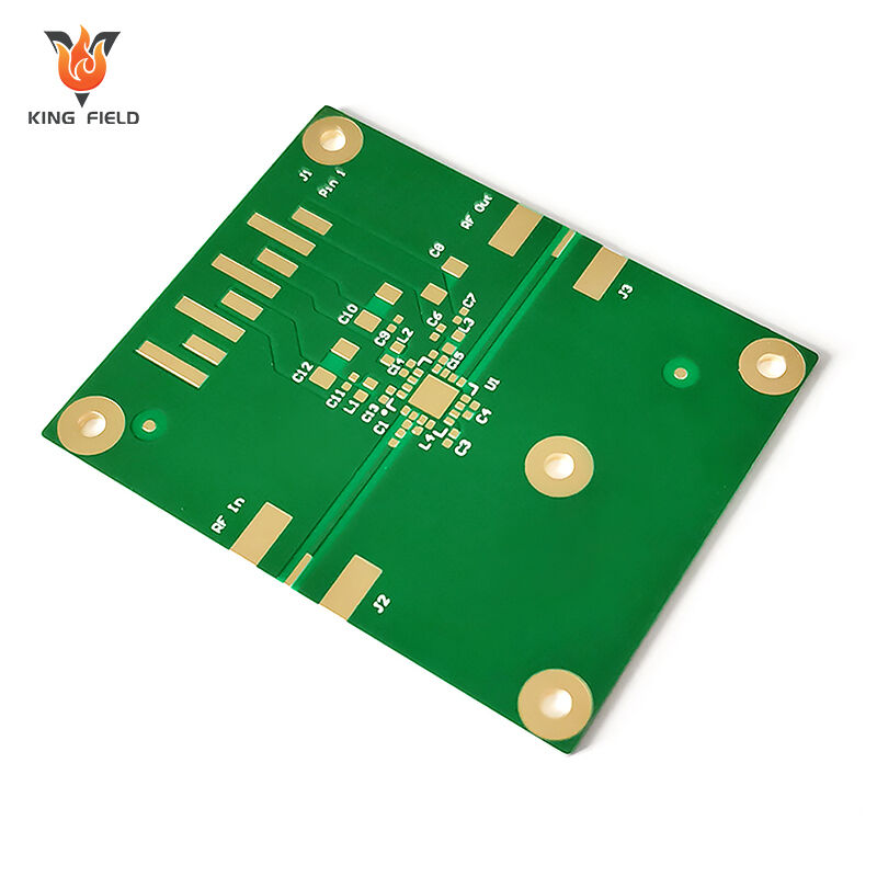
Un PCB constitue la structure squelettique — une carte inerte, fabriquée avec précision, qui fournit un support physique et les voies électriques nécessaires. Le PCB lui-même, constitué de couches de matériau époxy renforcé de fibre de verre et de cuivre conducteur, reste non fonctionnel en l’absence de composants électroniques. Il est comparable à un réseau autoroutier attendant le trafic.
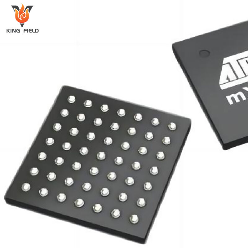
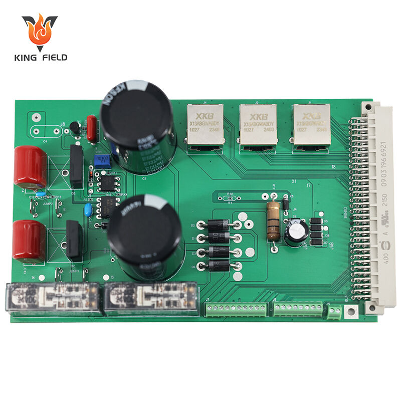
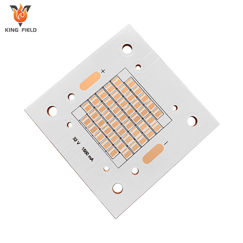
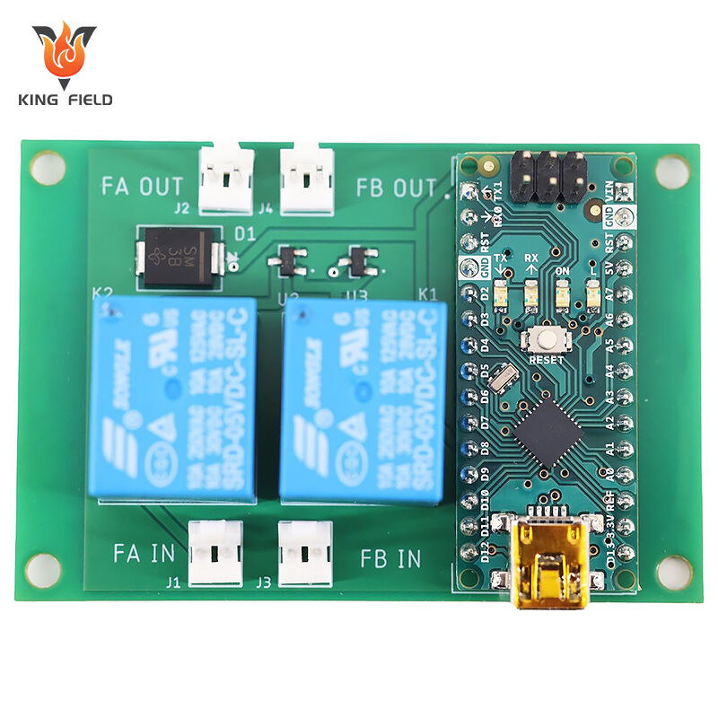
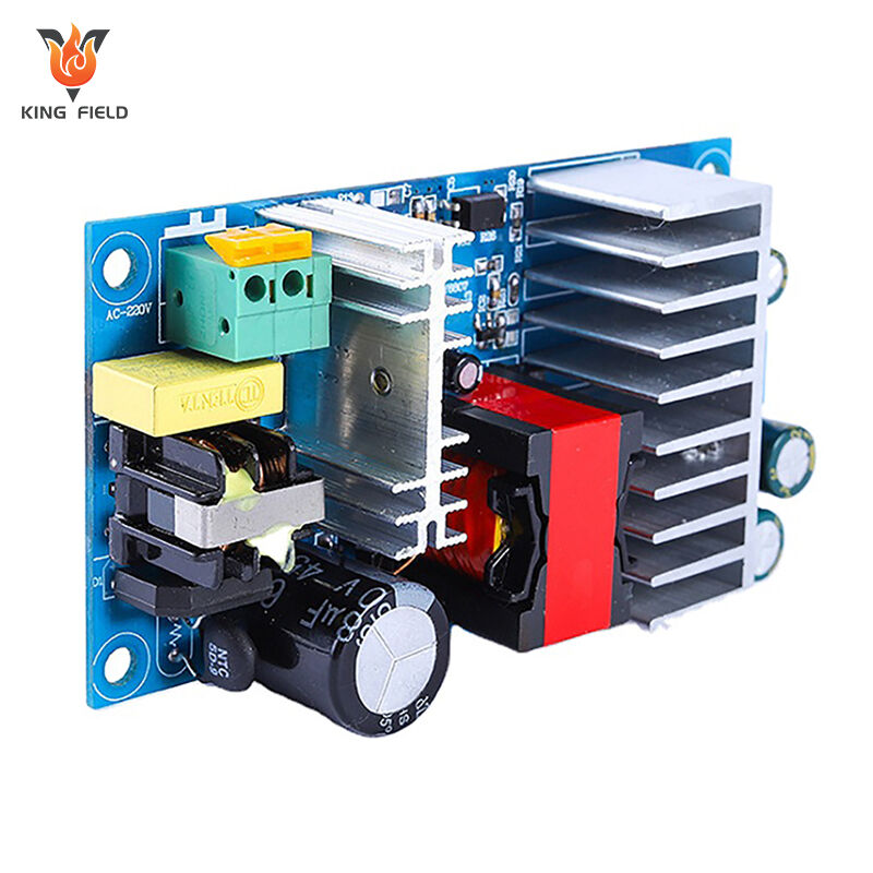
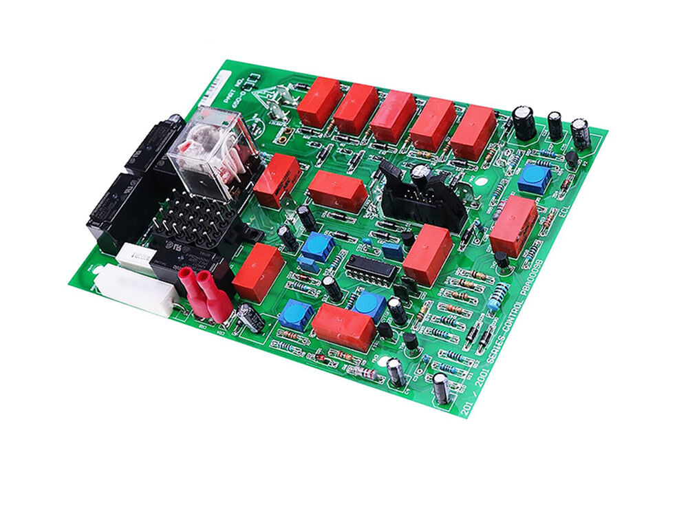
Une PCBA (carte de circuits imprimés assemblée), quant à elle, représente l’étape suivante du développement : il s’agit d’un circuit terminé, assemblé et fonctionnel. Ici, tous les composants électroniques passifs et actifs — tels que les résistances, les condensateurs, les diodes et les circuits intégrés (CI) — sont soudés avec précision sur la carte de circuits imprimés (PCB) à l’aide de techniques avancées telles que la technologie de montage en surface (SMT) ou la technologie de montage traversant (THT). La PCBA constitue les « cerveau, nerfs et organes » intégrés au « squelette » (PCB), transformant ce dernier en un sous-système électronique entièrement opérationnel.
Une carte de circuits imprimés (PCB) est le système fondamental présent dans presque tous les appareils électroniques actuels. Si vous avez déjà ouvert un ordinateur, un téléphone portable, une télécommande ou encore un four à micro-ondes, vous avez effectivement vu une PCB — généralement une plaque plane et rigide, verte, dotée de pistes de cuivre brillantes et percée d’ouvertures de fixation, de connecteurs et de marquages.
Au cœur de son fonctionnement, un circuit imprimé (PCB) est une carte électrique nue et non fonctionnelle, fabriquée à partir de matériaux isolants sur lesquels sont laminées des couches minces de cuivre. Ces couches de cuivre sont précisément façonnées pour former des pistes conductrices — l’équivalent de routes ou d’autoroutes destinées aux électrons — à l’aide de données de conception et de procédés de fabrication avancés. Contrairement aux circuits câblés manuellement d’antan, les circuits imprimés modernes simplifient et systématisent la réalisation des interconnexions électriques.
Les performances et la robustesse d’un circuit imprimé dépendent de la qualité de ses matériaux de base et de sa construction. Voici ce qui compose un circuit imprimé moderne :
|
Pièce |
Description |
Objectif |
|
Substrat |
Généralement du FR4, du polyimide pour les circuits imprimés flexibles, ou d’autres options. |
Assure la résistance mécanique et l’isolation électrique. |
|
Couches de cuivre |
Feuilles minces de cuivre laminées sur le substrat. |
Achemine les signaux électriques et l’alimentation. |
|
Masque de soudure |
Couche protectrice, généralement polymère verte, recouvrant les pistes en cuivre. |
Prévient les courts-circuits involontaires ainsi que l'usure, et assure la coloration. |
|
Sérigraphie |
Fine couche d'impression blanche. |
Étiquettes destinées au positionnement des composants, aux identifiants de suggestion, aux motifs de logo. |
|
Connecteurs latéraux |
Pads de contact plaqués or le long du bord de la carte. |
Relie la carte de circuit imprimé (PCB) à des prises externes ou à des systèmes de bus. |
|
Vias |
Petites ouvertures métallisées percées à travers une ou plusieurs couches de la carte. |
Fixe électriquement les couches de cuivre en sens opposés (avant/arrière). |
Après la procédure minutieuse de conception et de fabrication de la carte de circuit imprimé (PCB), la carte obtenue n’est encore qu’un cadre inerte — une « toile vierge » constituée de cuivre, de fibre de verre et d’efforts. Pour donner vie à cette base, nous entrons dans le domaine de l’assemblage de cartes de circuit imprimé (PCBA, ou Printed Circuit Board Assembly). Le PCBA est l’étape indispensable qui transforme la PCB en un véritable cerveau électronique fonctionnel.
Un ensemble de carte de circuit imprimé (PCBA) est une carte de circuit imprimé (PCB) sur laquelle tous ses composants électroniques — à la fois passifs et actifs — ont été correctement positionnés, fixés et soudés. Ce n’est qu’après cet assemblage que la carte devient un circuit fonctionnel, capable de s’allumer, de traiter des informations et d’accomplir des tâches concrètes.
Caractéristiques essentielles d’un PCBA :
Fonctionne comme le cerveau et les nerfs des appareils électroniques
Assure le traitement des signaux, la logique, les communications et la surveillance de l’alimentation
Offre un environnement physique et électrique optimisé pour la fiabilité — permettant une efficacité conforme aux exigences du marché et aux attentes des utilisateurs finaux
Le processus de fabrication d’un PCBA implique plusieurs opérations très contrôlées :
Application de pâte à souder : une fine couche de pâte à souder est déposée sur les pastilles destinées aux composants à l’aide d’un pochoir.
Positionnement des composants : Des outils automatisés à haute vitesse, pilotés par ordinateur, ou des opérateurs qualifiés positionnent chaque élément dans sa zone optimale, conformément aux fichiers de conception du circuit imprimé (PCB) de l’installation.
Soudage :
Soudage par refusion : La carte est soumise à un four de refusion, où une température précisément contrôlée fait fondre la pâte à souder, créant ainsi des liaisons mécaniques et électriques.
Soudage par vague : Les cartes sont déplacées au-dessus d’une vague de soudure liquide, assurant la liaison entre les broches des composants et les pastilles.
Analyse et contrôle qualité : Des méthodes avancées telles que l’inspection optique automatisée (AOI), l’analyse par rayons X (pour les boîtiers BGA) et l’inspection visuelle manuelle permettent de vérifier le positionnement des composants, la qualité des soudures et de détecter toute anomalie.
Essais fonctionnels : Une fois tous les composants montés, la carte subit des tests en-circuit (ICT) et des tests fonctionnels de circuit (FCT) afin de confirmer son bon fonctionnement — ce qui signifie qu’un circuit imprimé nu s’est véritablement transformé en une carte électronique assemblée (PCBA) fiable.
Examinons ce qui compose une carte PCBA complète. Chaque aspect contribue à ses capacités, sa fiabilité et sa facilité de fabrication.
|
CompoNent |
Description |
Rôle dans la PCBA |
|
Bare pcb |
Carte rigide ou flexible avec cuivre structuré |
Structure fondamentale et réseau de signaux |
|
Composants simples |
Résistances, condensateurs, inductances |
Gèrent le courant, la tension et le système de filtrage |
|
Composants actifs |
Circuits intégrés (CI), microcontrôleurs, diodes, transistors |
Permettent le traitement, la logique, la détection et l’amplification |
|
Connecteurs |
USB, adaptateurs latéraux, connecteurs, douilles |
Autoriser les interfaces électriques extérieures |
|
Soudure et flux |
Pâte à souder, barres, fils ; agent de changement |
Relier mécaniquement et électriquement les composants |
|
Finitions de surface |
ENIG, HASL, OSP, argent/plomb par immersion |
Protéger le cuivre et fournir des pastilles de soudure fiables |
|
Adhésifs |
colles époxy, colles durcissant sous UV |
Fixer des composants volumineux ou sensibles aux vibrations |
Efficacité : en intégrant avec expertise des composants haut de gamme et en garantissant des liaisons de soudure fiables, les cartes PCBA atteignent les objectifs d’efficacité requis par les applications actuelles — des appareils intelligents et des véhicules électriques (EV) aux scanners IRM et aux satellites.
Intégrité : Les fabricants de PCBA appliquent des contrôles qualité rigoureux — en utilisant l’analyse, le tri et la conformité aux normes telles que l’IPC-A-610 et l’ISO 9001 — afin de garantir la fiabilité du produit, même dans des environnements exigeants ou critiques pour la sécurité.
Évolutivité : Les méthodes de montage automatisées prennent en charge tout, des petits lots aux appareils produits en masse à grande échelle.
Le passage d’un circuit imprimé nu (PCB) à un PCBA (circuit imprimé assemblé) fonctionnel est déterminé par la méthode d’assemblage choisie. La méthode optimale influence la fiabilité, le coût, la miniaturisation et le marché d’application du produit. Chaque méthode répond à des exigences spécifiques liées à la conception du circuit — notamment la bande passante, la puissance, la résistance mécanique et les volumes requis.
Le montage en surface (SMT) est l’approche dominante pour la fabrication des cartes électroniques actuelles, qui sont à la fois très compactes et hautes performances. Le SMT a révolutionné l’électronique en rendant possible des architectures de circuits exceptionnellement denses ainsi qu’une automatisation avancée.
Type de composant : Composants montés en surface (CMS), dotés de petites discontinuités métallisées, sont placés directement sur les pastilles de cuivre.
Procédure d’assemblage :
Impression par pochoir : application de pâte à souder selon un motif précis sur les pastilles désignées.
Pick-and-place : des machines automatisées positionnent rapidement les CMS sur les pastilles recouvertes de pâte à souder, à l’aide des données issues des fichiers centroïdaux.
Soudures par refusion : la carte est introduite dans un four contrôlé ; la pâte à souder fond, assurant la fixation des composants.
Inspection optique automatisée (AOI) : des caméras détectent les mauvais positionnements, les courts-circuits, les composants manquants ou inversés, ainsi que les défauts de soudure.
Analyse par rayons X : pour les boîtiers BGA et les dispositifs à joints cachés, l’imagerie radiographique permet de vérifier la solidité des liaisons.
Miniaturisation poussée.
Configuration à haute vitesse et en grand volume.
Capacité d’installation d’éléments des deux côtés.
Amélioration des performances électriques grâce à la réduction des dimensions des pistes et de l’inductance.
Applications SMT classiques :
Appareils numériques grand public.
Équipements à haute vitesse.
Électronique médicale et automobile, où l’épaisseur est critique.
La technologie des composants traversants (THT) est la première méthode d’assemblage et demeure essentielle pour les applications exigeant une résistance mécanique et une durabilité optimales.
Type d’élément : les broches (jambes) s’étendent à travers des ouvertures percées dans la carte de circuit imprimé (PCB).
Configuration du processus de soudage par vague :
Insertion des composants : les éléments sont insérés manuellement ou à l’aide d’outils semi-automatiques directement dans les ouvertures correspondantes de la carte.
Soudage par vague : les cartes passent sur une « vague » de soudure liquide, qui remonte à travers les ouvertures afin de souder les broches et les pastilles.
Rabattage des broches et nettoyage : les broches excédentaires sont coupées ; les résidus de flux sont éliminés.
Liaisons mécaniques plus robustes ; idéal pour les composants volumineux ou lourds.
Fiabilité supérieure dans des environnements à forte vibration ou sévères.
Plus facile à réparer manuellement, à prototyper et à configurer pour des productions de faible volume ou personnalisées.
Applications THT classiques :
Aérospatiale, militaire et électronique automobile.
Dispositifs électroniques de puissance, transformateurs, ports, relais.
Commandes industrielles soumises à des chocs, à des résonances et à des extrêmes de température.
L’assemblage hybride utilise à la fois la technologie SMT et la technologie THT, tirant parti des avantages de chaque méthode.
Les cartes de circuits imprimés nécessitent souvent des composants SMT pour les circuits numériques ou de communication denses, et des composants THT pour les connecteurs robustes, les transformateurs ou les composants dissipant de la chaleur.
Permet une combinaison adaptable : par exemple, un contrôleur de drone peut utiliser des circuits intégrés et des capteurs SMT, ainsi que des composants THT pour les prises d’alimentation et les condensateurs de grande capacité.
Les composants SMT sont créés et soudés initialement (reflow).
Les composants THT doivent être insérés manuellement puis soudés par vague.
Les cartes finales peuvent subir une inspection combinée et des tests en plusieurs étapes.
Bien que les termes PCB et PCBA soient parfois utilisés de façon interchangeable, ils désignent en réalité des étapes distinctes du processus de fabrication d’appareils électroniques, chacune possédant ses propres caractéristiques fonctionnelles, coûts, exigences techniques et applications sur le marché.
PCB (carte de circuits imprimés) : Le PCB est une structure organisée, non fonctionnelle — une carte de câblage vide constituée de couches de substrat (par exemple FR4), de pistes en cuivre, de masque de soudure et d’impression sérigraphique. Sa fonction est de fournir un support mécanique et des voies électriques pour les composants à venir, sans toutefois fonctionner comme un circuit en soi.
PCBA (assemblage de carte de circuits imprimés) : Le PCBA est la carte terminée — essentiellement, la carte de circuits imprimés (PCB) sur laquelle tous les composants électroniques requis (passifs et actifs) ont été placés et soudés. À ce stade, la carte constitue un module électronique fonctionnel capable d’effectuer des calculs, d’assurer des fonctions de commande, d’interaction, de surveillance de l’alimentation ou de détection.
Conseils pour la fabrication de cartes de circuits imprimés (PCB) :
Format : conception CAO, génération des fichiers Gerber.
Fabrication : préparation du substrat, laminage du cuivre, gravure du motif, perçage, métallisation, application du masque de soudure, impression sérigraphique, finition de surface et inspection finale.
Conseils pour la fabrication de PCBA :
Préparation à l’assemblage : nomenclature (BOM), données de pose automatique (pick-and-place) et de centroïde, approvisionnement des composants.
Montage des composants : technologie de montage en surface (SMT) et/ou technologie de montage traversant (THT).
Soudage : reflow (SMT), soudage par vague (THT).
Évaluation et tests : inspection optique automatisée (AOI), radiographie X, test in-circuit (ICT), test fonctionnel (FCT), vérifications pratiques.
|
Aspect |
CFP |
PLCBA |
|
Fonction |
Plinthe inerte |
Circuit électronique entièrement fonctionnel. |
|
Conception axée sur le design |
Transfert des pistes, empilement des couches, conception pour la fabrication (DFM) |
Type de composant, stratégie de soudage, tri |
|
Personnalisation |
Matériau des couches, matériau, finition |
Choix des composants, micrologiciel, configuration en série |
|
Examen des besoins |
Test électrique, continuité, courts-circuits |
Test en circuit, test fonctionnel, test environnemental, inspection optique automatique (AOI), radiographie |
|
Réparabilité |
Certains (traces de découpe/saut) |
Installation (nécessite un dessoudage, peut endommager les pastilles) |
Carte de circuits imprimés (PCB) : coût faible à modéré par unité ; déterminé principalement par les dimensions de la carte, le nombre de couches, le produit et le revêtement. Idéale pour l’automatisation et la réalisation de prototypes.
Carte de circuits imprimés assemblée (PCBA) : coût système plus élevé ; inclut les coûts liés à :
L’achat des composants.
La main-d’œuvre ou l’automatisation de l’assemblage.
La surveillance et le contrôle qualité.
Les pertes liées aux problèmes survenus lors de la mise en service.
Les procédures incluses comprennent le nettoyage, l’évaluation et l’emballage du produit.
PCB : Délai le plus rapide (seulement 24 à 72 heures pour les versions express ou 1 à 2 semaines pour les fabrications classiques, selon la complexité).
PCBA : Délai plus long, généralement de 2 à 4 semaines ou plus, en raison des chaînes d’approvisionnement, de l’organisation de l’assemblage et des contrôles post-assemblage.
PCB : Livrés sous forme de cartes vierges ; utilisés par les ingénieurs pour la phase de prototypage ou dans les entreprises disposant de leur propre chaîne de production.
Conditionnement : Sous vide, empilables, anti-humidité.
PCBA : Livrés prêts à l’intégration, sous forme de composants finis ; utilisés dans la fabrication finale, prêts pour l’intégration dans un environnement ou un système.
Conditionnement : Compartimenté, antistatique, souvent réalisé sur mesure à l’aide de bacs protégeant les composants sensibles.
Les PCB sont privilégiés lorsque :
Au début du cycle de vie du produit (prototypage, recherche et développement).
Les entreprises souhaitent se créer ou se transformer.
Des coûts préliminaires de production minimisés sont requis.
Les cartes de circuits imprimés assemblées (PCBA) sont privilégiées lorsque :
Des solutions complètes sont privilégiées (externalisation de la complexité).
Un délai court pour la mise sur le marché est essentiel.
Des installations, des circuits de haute qualité ou à haute vitesse sont requis.
Les compétences ou les équipements nécessaires ne sont pas disponibles en interne.
Les cartes de circuits imprimés (PCB) et les cartes de circuits imprimés assemblées (PCBA) représentent des étapes successives et complémentaires du processus de fabrication d’appareils électroniques — une relation de collaboration au cœur de chaque produit numérique intelligent.
Une carte PCB constitue l’élément de départ de tout type d’appareil électronique moderne. Elle remplit les fonctions suivantes :
Structure mécanique — définissant la disposition et le positionnement des composants.
Réseau interconnecté — déterminant les voies électriques destinées aux signaux et à l’alimentation.
« Toile » de conception — sur laquelle toute la chaîne de production ultérieure placera, soudera et testera les composants.
Une carte PCBA est obtenue lorsqu’une carte PCB nue est équipée de tous ses composants électroniques requis, à l’aide de techniques d’assemblage telles que la technologie de montage en surface (SMT), le montage traversant (THT) ou une combinaison des deux.
Dépendances clés :
Une PCBA ne peut être assemblée sans sa carte PCB : le substrat, les pistes en cuivre, les vias et les pastilles de soudure présents sur la carte PCB constituent des supports essentiels pour chacun des composants électroniques durant l’assemblage.
La précision, la propreté et la qualité matérielle de la carte PCB influencent directement la soudabilité, l’intégrité électrique et la fiabilité à long terme de la carte PCBA.
Focus : Empilement des couches, intégrité du signal, résistance mécanique.
Résultat : Carte vide non fonctionnelle, mais testable.
Accent mis sur : Sélection des composants, positionnement précis, soudure durable et tests approfondis.
Résultat final : Circuit pratique — prêt à être intégré directement dans un produit fini.
Carte PCB : Généralement sous vide, chargée et classée — risque très faible, transport extrêmement aisé.
Carte PCBA : Nécessite un emballage personnalisé antistatique et compartimenté afin de protéger les composants délicats et les joints de soudure sensibles contre les décharges électrostatiques (ESD), les manipulations et les vibrations.
La fabrication des cartes PCB constitue généralement la base modulaire d’une chaîne d’approvisionnement, ce qui permet une grande flexibilité : diverses conceptions ou spécifications de cartes PCB pour différents modèles ou besoins clients personnalisés.
L'établissement de PCBA consiste à séparer, inspecter et ajouter de la valeur aux composants — ce qui soutient aussi bien la réalisation rapide de prototypes que les solutions finales destinées aux équipementiers d'origine (OEM) du grand public.
Les cartes de circuits imprimés (PCB) et les ensembles de cartes de circuits imprimés (PCBA) constituent la structure physique et fonctionnelle de l’ère des appareils numériques. Leur simplicité, leur évolutivité et leur personnalisation ont rendu possibles des innovations sans précédent dans de nombreux domaines technologiques. Que ce soit sous la forme d’une carte simple à simple face ou d’un assemblage multicouche entièrement garni et à haute densité, ces fondations sont devenues essentielles dans presque tous les secteurs.
Les PCB et les PCBA se trouvent au cœur des appareils grand public modernes — où densité, rentabilité et hautes performances sont essentielles.
Avantages courants des PCBA :
Téléphones intelligents et tablettes : les PCBA multicouches gèrent l’alimentation, le traitement, les capteurs, les communications et les antennes dans des espaces ultra-minces.
Ordinateurs portables et ordinateurs domestiques : Cartes mères complexes avec des composants SMT et THT très denses, prenant en charge des processeurs rapides, de la mémoire et des entrées/sorties.
Appareils portables : Cartes imprimées assemblées (PCBA) ultra-minuscules et adaptables, conçues pour optimiser le confort, l’autonomie de la batterie et les communications sans fil.
Appareils électroménagers et loisirs : Cartes à double face ou multicouches pilotant les circuits de commande des téléviseurs, des machines à laver, des unités de climatisation, des enceintes audio intelligentes, et bien plus encore.
La tendance vers l’électrification, l’automatisation et la connectivité des camions repose sur des solutions robustes et fiables de cartes de circuits imprimés (PCB) et de cartes imprimées assemblées (PCBA).
Applications confidentielles incluent :
Unités de commande moteur (ECU) / Commande de transmission : PCBAs multicouches répondant à des exigences strictes en matière de température, de résistance aux vibrations et de compatibilité électromagnétique (CEM).
Gestion des batteries pour véhicules électriques (VE) : PCBAs à forte teneur en cuivre destinées à la gestion du courant, à la sécurité et à la protection.
Systèmes avancés d’aide à la conduite (ADAS) : Configurations multicouches haute vitesse, optimisées pour les fréquences radio (RF), destinées aux radars, aux caméras numériques et à l’intégration des systèmes de détection.
Infomercial et navigation : cartes complexes dotées de fonctionnalités HDMI, GPS, Bluetooth et d’une interface utilisateur évoluée.
L’automatisation industrielle, la robotique et les systèmes de commande exigent des cartes de circuits imprimés assemblées (PCBA) robustes, fiables et conçues pour des environnements sévères.
La sécurité et la précision sont primordiales dans le domaine de la santé, aussi les PCBA doivent-elles répondre aux exigences les plus strictes en matière d’intégrité et de biocompatibilité.
Les dispositifs informatiques performants reposent sur des PCBA à haute vitesse et multicouches afin de supporter des interconnexions denses pour le traitement, la mémoire et la distribution d’énergie.
L’infrastructure de télécommunications repose sur des PCBA capables de gérer des signaux haute fréquence, à faibles pertes, tout en assurant une dissipation thermique sûre et fiable.
Conditions d’utilisation typiques :
Stations de base, commutateurs, routeurs : cartes multicouches optimisées RF assurant une interaction ultra-rapide et sans erreur.
Composants sans fil : PCBAs compactes et sécurisées pour les éléments 5G/LTE, Wi-Fi et Bluetooth.
Dans les domaines de l’aérospatiale, de la défense et des technologies satellitaires, les PCB/PCBAs sont soumis à certains des environnements fonctionnels les plus exigeants au monde.
Principales applications :
Systèmes de cockpit et d’avionique : cartes rigides-flexibles et durcies contre les radiations, garantissant une intégrité absolue et une réduction du poids.
Systèmes satellitaires : PCBAs légères, résistantes aux températures extrêmes et qualifiées pour les vibrations, destinées au traitement des signaux et à la télémétrie.
Systèmes de guidage, de projectiles et de radars : ensembles ultra-résistants comportant des pistes blindées répétées et des traitements avancés de blindage.
La miniaturisation, l’efficacité énergétique et la longévité sont les principaux moteurs de la conception des PCB/PCBAs pour l’Internet des objets.
Applications mises en évidence :
Prélèvement à distance d’appareils et de balises intelligentes : PCBAs polyvalentes, minuscules et à très faible consommation d’énergie, pour une localisation et une utilisation de la batterie extrêmement réduites.
Composants pour la maison intelligente : Cartes double face ou simple face destinées aux boutons, aux capteurs environnementaux et aux contrôleurs.
Internet des objets industriel (IoT industriel) : Cartes imprimées robustes destinées à la collecte et au contrôle de données sur le terrain.
Le choix entre la fabrication de cartes imprimées nues (PCB) et une solution PCBA entièrement assemblée constitue une décision cruciale dans le cycle de vie des dispositifs électroniques. Cette décision influence les coûts, les délais, les besoins en validation, la complexité de la chaîne d’approvisionnement et, inévitablement, le succès de votre projet. Le meilleur choix dépend de vos ressources techniques, de votre volume de production, de vos délais et de votre méthode de gestion des risques.
Les prestataires de services de cartes imprimées nues sont privilégiés lorsque vous :
Vous trouvez encore en phase de prototypage ou de conception très précoce : Vous pouvez ainsi itérer rapidement sur les schémas de circuits et tester concrètement la connectique standard ou l’ajustement dans un espace système.
Posséder une capacité interne d'assemblage d'appareils électroniques : accès aux procédés de soudage par reflow ou par vague, stations de soudage manuel et ingénieurs/techniciens expérimentés.
Nécessiter un contrôle total sur l’approvisionnement des composants : souhaiter sélectionner, évaluer ou remplacer les distributeurs pour chaque composant individuel.
Souhaiter améliorer les coûts grâce à une moindre implication en matière d’infrastructure ou de R&D : économiser sur les frais de mise en place et de distribution — notamment pour les productions à faible volume ou les réalisations unitaires.
Les solutions PCBA fournissent une carte mère entièrement fonctionnelle et prête à l’emploi. Elles sont particulièrement adaptées lorsque vous :
Avez besoin d’un service complet prêt pour la production : les prestataires PCBA se chargent de l’approvisionnement de tous les composants, de l’assemblage complet, des tests et offrent un système opérationnel — simplifiant ainsi considérablement votre processus.
Ne disposez pas d’équipements internes ou d’expérience en montage : pas de ligne SMT ? Pas de terminaux THT ? Externalisez cette activité auprès d’experts et concentrez-vous sur vos compétences fondamentales, telles que la conception produit, le développement logiciel ou le marketing.
Configuration très spécialisée ou à forte densité requise : les installations SMT, BGA ou les composants à pas fin nécessitent des équipements innovants de pose et d’évaluation par rayons X, qui ne sont pas disponibles dans de nombreux laboratoires de développement.
Souhaitez réduire la complexité de la chaîne d’approvisionnement : moins de fournisseurs, moins d’accords, moins de déceptions liées au contrôle qualité. Logistique structurée et moindres risques d’arrêts de production.
Vous devez accélérer le délai de mise sur le marché : concentrez-vous sur l’expédition des produits aux clients ou sur le passage à une production à grande échelle, sans courir le risque de défauts ou de cycles imprévus de reprise en main.
|
Facteur |
Bare pcb |
PCBA (clé en main) |
|
Phase du produit |
R&D, prototype, banc d’essai |
Prêt pour la production, lancement en série |
|
Ressources techniques requises |
Soudure, contrôle interne |
Minimal, géré par le représentant |
|
Coût |
Le plus faible pour les projets simples |
Dépenses système plus élevées, main-d’œuvre, assurance qualité |
|
Délai de livraison |
Court (1 à 7 jours courants) |
Plus long (en raison de l’approvisionnement et de la mise en place) |
|
Risque / Complexité |
Erreurs manuelles lors de la configuration, risque DFM |
Le fournisseur s’occupe de la configuration et du DFM |
|
Flexibilité |
Le plus élevé pour les ajustements / retravaux |
Idéal pour les commandes répétées et l’augmentation des volumes |
|
Test |
À faire soi-même ou sous-traité |
AOI, ICT et FCT complets |
|
Cas d'utilisation |
Bidouillage et prototypage personnels |
Lancement commercial, marchés contrôlés |
La qualité supérieure et la fiabilité de vos appareils électroniques dépendent de l'expérience et des compétences de vos partenaires de production. Quelle que soit la solution retenue, assurez-vous que votre fournisseur remplit bien ces critères :
Conformité IPC : respect des normes IPC-A-600 (exigences relatives aux cartes PCB) et IPC-A-610 (normes relatives aux cartes PCBA), garantissant une fabrication durable et une constance élevée.
Certifications : recherchez les certifications ISO 9001 (management de la qualité), ISO 13485 (dispositifs médicaux), IATF 16949 (automobile) ou d'autres autorisations spécifiques au secteur.
Capacités complètes : solutions « clé en main » (conception, fabrication, montage, tests, logistique) permettant une résolution rapide des problèmes et optimisant la conception pour la fabrication (DFM).
Devis et communication clairs : Une gestion claire de la nomenclature (BOM), des vérifications DFM, un CRM robuste et une assistance technique rapide sont des signes d’un centre de production bien organisé et digne de confiance.
Références (Étude) : Recommandations issues de projets ou de marchés similaires, avec des taux de résolution éprouvés et vérifiés ainsi qu’une livraison ponctuelle.
Choisissez des cartes PCB nues lorsque la souplesse, la réalisation de prototypes ou l’ajustement des composants constituent vos principales préoccupations.
Optez pour des cartes PCBA lorsque le délai de mise sur le marché, l’évolutivité, la fiabilité ou la simplification de la chaîne d’approvisionnement revêtent une importance capitale.
Approche hybride : Certaines entreprises utilisent des cartes nues en phase de conception, puis passent à une solution clé en main (PCBA) pour les dernières séries pilotes ou de production. Cette stratégie réduit les risques liés à la conception et permet un développement stratégique échelonné.
Le choix du partenaire de fabrication idéal pour vos cartes de circuits imprimés (PCB) ou vos cartes assemblées (PCBA) ne repose pas uniquement sur le prix ou la préparation — il s’agit surtout de réduire les risques, d’assurer la qualité du produit et de garantir la sécurité durable de votre chaîne d’approvisionnement. Le fabricant que vous sélectionnez influencera le délai de mise sur le marché de votre projet, le taux de défauts, la conformité réglementaire et votre capacité future à l’adapter à des volumes accrus.
Pour éviter des problèmes coûteux, voici une démarche structurée permettant de choisir un fournisseur fiable de PCB ou de PCBA.
Ancienneté dans le secteur et expertise spécifique dans votre niche : les fournisseurs disposant d’un historique éprouvé dans votre domaine comprennent vos besoins particuliers, les problèmes courants auxquels vous êtes confrontés ainsi que les obstacles liés à la conformité.
Plage de volumes : ce fournisseur est-il capable de passer de la fabrication de prototypes à la production en série ? Propose-t-il des séries courtes ou des quantités minimales de commande (QMC) adaptées à vos besoins ?
Côté PCB :
Nombre de couches (jusqu’à 32 couches ou plus pour les applications haute densité ou haute vitesse).
Substrats avancés (par exemple FR4, polyimide, Rogers, céramique, noyau métallique).
Guidage en lignes fines, microvia, via enterrées/aveugles.
Surfaces spécifiques (ENIG, immersion argent/étain, or difficile, OSP).
Cartes rigides, flexibles et rigides-flexibles.
Côté PCBA :
Capacités SMT et THT (y compris pas fin, BGA, QFN, modules PoP).
Inspection optique automatisée (AOI) et radiographie pour les BGA.
Tests utiles et tests en circuit (ICT, FCT).
Prototypage avancé (délai rapide) et lignes à forte volumétrie.
Certifications obligatoires :
ISO 9001 : Système général de management de la qualité premium.
IPC-A-600 / IPC-A-610 : Exigences relatives à la qualité de fabrication et d’assemblage des cartes de circuits imprimés (PCB) et des cartes assemblées (PCBA).
Conformité UL, RoHS, REACH : Lorsque la sécurité ou le contrôle du statut est requis.
ISO 13485, IATF 16949, AS9100 : Spécifiquement destinées aux marchés clinique, automobile et aérospatial.
Équipements d’assurance qualité :
Évaluation des produits entrants (IQC).
Inspection optique automatisée (AOI), radiographie (X-ray), test en circuit (ICT) et contrôles finaux d’assurance qualité à diverses étapes du processus.
Traçabilité complète (numéros de lot, suivi des composants, intégration MES/ERP).
Systèmes d’amélioration continue et de retour d’information.
Approvisionnement des pièces : Votre représentant dispose-t-il de contacts vérifiés auprès de fournisseurs fiables ? Est-il en mesure de gérer les problèmes liés aux quantités et à l’obsolescence ?
Gestion des menaces liées aux contrefaçons : Des systèmes rigoureux d’approvisionnement, de vérification et de traçabilité réduisent le risque d’utilisation de pièces contrefaites ou de qualité inférieure.
Gestion complète de la nomenclature (BOM) : Assistance de bout en bout — gestion des pièces obsolètes, approvisionnement diversifié, optimisation des délais de livraison et maîtrise de l’approvisionnement.
Le fabricant est-il capable de fournir des échantillons en quelques jours et de passer à la production en quelques semaines ?
Gère-t-il efficacement les commandes à délai très court et les modifications de conception (ordres de changement d’ingénierie, ECO) ?
Quantités minimales commandables adaptables afin de s’aligner sur votre croissance et le cycle de vie de vos produits.
Superviseurs de comptes dédiés, assistance réactive par e-mail/téléphone/chat.
Interlocuteurs techniques ou développeurs anglophones, en cas d’approvisionnement à l’échelle mondiale.
Mises à jour typiques sur l’état des jalons de production et le suivi des expéditions.
Conception pour la fabrication (DFM) et assistance en matière d’agencement afin d’optimiser les formats avant la fabrication ou la mise en place.
Outils de devis tarifaires en ligne : coûts en temps réel, simulation de préparation et réponses techniques concernant les devis pour cartes PCB et assemblages PCBA.
Transparence des coûts : décomposition complète des frais. Méfiez-vous des frais imprévus !
Témoignages favorables sur des plateformes de marché indépendantes, confirmés idéalement par des références directes.
Assistance après-vente pour les retours, la garantie ou la résolution de problèmes techniques.
Engagement à signer des accords de confidentialité (NDA) ou à protéger votre propriété intellectuelle — particulièrement crucial pour les produits innovants ou uniques.
Vous trouverez ici des solutions claires aux préoccupations les plus courantes des ingénieurs, des responsables produit et des professionnels des achats concernant les cartes de circuits imprimés (PCB) et les cartes assemblées (PCBA). Ce guide peut vous servir de référence rapide pour éviter les écueils et prendre des décisions éclairées.
Les PCB (cartes de circuits imprimés) sont des cartes nues — non fonctionnelles tant que les composants électroniques n’y ont pas été intégrés. Elles assurent un support mécanique et des voies électriques, mais ne s’allument pas ni ne traitent de signaux par elles-mêmes.
Les PCBA (cartes de circuits imprimés assemblées) sont des modules terminés et opérationnels — c’est-à-dire une PCB sur laquelle tous les composants ont été soudés, entièrement testée et prête à être intégrée dans un système.
PCB nue : La fabrication express de PCB peut être réalisée en 1 à 7 jours pour les modèles simples, et en 5 à 15 jours pour les cartes multicouches de complexité moyenne à élevée, en série.
PCBA : Généralement 2 à 6 semaines à compter de la soumission des fichiers. Le délai pour les PCBA varie considérablement, en fonction de :
Temps d’approvisionnement de tous les éléments de la nomenclature (BOM).
Configuration du PCBA.
Séquençage de l’assemblage, inspection et tests fonctionnels.
Réaliste : Si le « délai de mise sur le marché » est crucial, privilégiez une solution complète incluant un approvisionnement fiable des composants et une expertise en assemblage afin d’éviter les retards liés aux composants ou les erreurs de planification.
Techniquement possible, mais fortement déconseillé. Le retrait des composants soudés — « démontage » d’un PCBA — peut :
Endommager les pastilles ou les pistes, notamment sur les cartes multicouches ou à pas fin.
Laisser des résidus de soudure, ce qui augmente le risque de problèmes futurs.
Provoquer une déformation si la carte est soumise à plusieurs cycles de températures élevées.
Technique optimale : Réutiliser des cartes de circuits imprimés uniquement à des fins d’étude de conception, de réparation de circuits ou de « criblage destructif ». Les produits essentiels doivent toujours utiliser des cartes neuves afin de garantir leur fiabilité.
Respectez les normes du secteur en matière de largeur des pistes, d’espacement, de dimensions des trous, de dégagements entre composants et de format des pastilles — consultez le tableau des capacités de votre fabricant sous-traitant (CM).
Utilisez les outils de vérification des règles de conception (DRC) et d’évaluation DFM intégrés à votre logiciel CAO ou fournis par votre partenaire de production.
Une collaboration précoce avec votre distributeur de cartes de circuits imprimés / cartes assemblées (PCB/PCBA) permet d’obtenir des commentaires sur la conception avant de vous engager dans des conceptions coûteuses ou à risque.
Oui ! De nombreux fabricants modernes proposent des services intégrés couvrant la fabrication des cartes (fab), l’approvisionnement des composants, le montage et même la fabrication des bacs de test.
Avantages :
Interaction structurée.
Gestion des changements plus rapide (ECO).
A tiré le meilleur parti de la conception pour la fabrication.
Contrôle / traçabilité haut de gamme de bout en bout.
 Actualités en vedette
2026-04-18
2026-04-17
2026-04-13
2026-04-12
2026-04-11
2026-04-10
2026-04-09
2026-04-06