Collegamenti rapidi
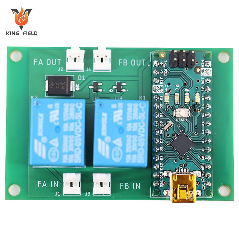
Le schede a circuito stampato (PCB) costituiscono la base fondamentale di praticamente ogni strumento elettronico, dai dispositivi clinici salvavita ai sistemi avanzati di assistenza alla guida (ADAS) nelle automobili, fino ai dispositivi elettronici di consumo, agli strumenti aerospaziali e all'automazione industriale. Nell'attuale era della produzione su larga scala, le aspettative riguardo all'integrità delle PCB e alla produzione esente da difetti non sono mai state così elevate. Gli impianti di produzione di massa, in particolare nel settore automobilistico, professionale e aerospaziale, richiedono test avanzati sulle PCB, ispezioni approfondite delle PCB e solide metodologie di controllo qualità per mitigare i rischi, ridurre i costi di produzione e garantire prestazioni eccezionali delle schede.
L'aumento della complessità degli articoli, la riduzione delle geometrie e le pressioni normative rendono fondamentale adottare sistemi di rilevamento dei difetti basati sulle migliori pratiche, acquistare ispezione ottica automatica (AOI), test in-circuit (ICT), test funzionali e screening con sonda volante, nonché perseguire un continuo ripristino del processo.
L'affidabilità delle PCB è una misura di quanto costantemente una scheda a circuito stampato possa svolgere la propria funzione elettrica prevista, nelle condizioni operative e ambientali attese, per l'intera durata di vita prevista, senza subire guasti. Le PCB ad alta affidabilità sono progettate non solo per funzionare, ma per funzionare perfettamente anche in presenza di sollecitazioni ripetute:
Cicli termici.
Sollecitazioni meccaniche.
Tensione elettrica.
Esposizione diretta all'ambiente.
Le PCB ad alta affidabilità costituiscono la base di sistemi critici per la missione, nei quali un guasto può portare a conseguenze disastrose. Si considerino gli esiti potenziali in questi scenari:
Dispositivi elettronici per autoveicoli / ADAS: una scheda a circuito stampato (PCB) difettosa nei sistemi di avviso di separazione delle corsie, di prevenzione degli incidenti o negli elementi radar può mettere a rischio vite umane e compromettere la credibilità di un marchio.
Dispositivi medici: errori di progettazione o produzione su una PCB possono ostacolare dispositivi per l’imaging scientifico, il supporto vitale o il monitoraggio, mettendo in pericolo la sicurezza e l’incolumità dei pazienti.
Aerospaziale e controllo industriale: malfunzionamenti possono causare costosi tempi di fermo, danni materiali o l’arresto completo del sistema.
Garantire la realizzazione di PCB ad alta affidabilità nell’ambito dell’automazione richiede una comprensione fondamentale dei fattori che influenzano maggiormente sia l’efficacia iniziale sia la robustezza a lungo termine. Dalle fasi di produzione della PCB al posizionamento dei componenti e ai sistemi avanzati di rilevamento dei difetti, ogni fase comporta potenziali rischi di insuccesso — oppure opportunità per miglioramenti di eccellenza qualitativa. Esaminiamo i principali fattori:
Il viaggio verso l'affidabilità della PCB inizia a livello molecolare. La scelta del materiale per la PCB determina semplicemente come la vostra scheda madre gestirà i carichi termici, le sollecitazioni elettriche, l'esposizione ambientale e le pressioni meccaniche.
Sicurezza termica: Il normale FR-4 è adatto alla maggior parte delle applicazioni, ma l'elettronica automobilistica e aerospaziale più esigente potrebbe richiedere materiali ad alta temperatura di transizione vetrosa (high-Tg) o poliimide. Le schede in poliimide mantengono l'affidabilità durante cicli prolungati di variazione della temperatura, offrendo al contempo un'eccellente resistenza alla fiamma.
Assorbimento di umidità: Un'eccessiva umidità può compromettere i legami, causare delaminazione, favorire la corrosione e aumentare la conducibilità superficiale, provocando cortocircuiti nascosti. I materiali con un assorbimento di umidità ridotto sono più adatti per ambienti umidi.
Inelasticità meccanica: Le schede soggette a vibrazioni, flessione o urti devono avere lo spessore e l’aspetto estetico del prodotto adeguati — comunemente stack ibridi o laminati rinforzati — per ridurre la rottura delle piste e il guasto dei giunti saldati.
La qualità inizia già con la scheda di ingresso. La fase di definizione del formato della PCB deve garantire efficienza elettrica, realizzabilità produttiva e copertura dei test. Errori o omissioni in questa fase si ripercuotono sull’intero processo successivo.
Stabilità del segnale e distribuzione dell’alimentazione: utilizzare percorsi corti e lineari per i segnali ad alta frequenza/alta potenza al fine di ridurre le interferenze elettromagnetiche (EMI) e le cadute di tensione.
Gestione termica: integrare vie termiche, dissipatori di calore e ampie aree di rame sotto i componenti generanti calore.
Posizionamento efficace dei componenti:
Posizionare i condensatori di disaccoppiamento il più vicino possibile ai pin di alimentazione per ridurre gli sbalzi di tensione.
Raggruppare i componenti per dominio funzionale.
Posizionare i componenti sensibili alle vibrazioni nelle vicinanze dei supporti della PCB o dei fori di fissaggio.
Stile per la testabilità (DFT):
Pianificare i punti di verifica e garantire l'accesso in profondità durante la progettazione, assicurando che tutti i circuiti critici possano essere verificati mediante test ICT o a sonda volante.
Aggiungere punti di contatto integrati per le dimostrazioni e la valutazione del firmware.
Distanze di isolamento e distanze di strisciamento: mantenere distanze sicure tra piste, pad e tagli laterali — in particolare in configurazioni ad alta tensione, ad alta corrente o esposte a contaminazione.
Routing controllato dell’immunità: nelle applicazioni ad alta velocità/ADAS, progettare coppie differenziali e piste schermate per preservare la qualità del segnale.
Anche la migliore progettazione di PCB può essere compromessa da una produzione frettolosa o non uniforme. Il controllo di processo è il fondamento di una produzione di schede ripetibile e affidabile.
Applicazione precisa della pasta saldante: un allineamento accurato del pattern e un controllo preciso della quantità di pasta evitano ponticelli di saldatura e connessioni aperte.
Posizionamento automatico dei componenti: i dispositivi ad alta velocità per il prelievo e il posizionamento garantiscono un’accuratezza continua anche per gli elementi più piccoli, riducendo al minimo i componenti mal posizionati, che spesso causano problemi nelle schede a circuito stampato (PCB) per sistemi ADAS e strumenti medici.
Profili di rifusione completamente ottimizzati: la temperatura e i tempi di saldatura devono essere adeguati sia alla complessità della scheda sia al tipo di pasta saldante, per evitare giunzioni difettose o surriscaldamento.
Ispezione ottica automatica (AOI): l’esame estetico in tempo reale garantisce la qualità delle giunzioni saldate, la corretta polarità dei componenti e l’assenza di difetti superficiali direttamente lungo la linea di produzione.
Verifica in-circuito e funzionale: questi sistemi automatizzati eseguono misurazioni su ogni punto di controllo confermato, consentendo di individuare errori non rilevabili tramite AOI, come circuiti aperti o valori errati dei componenti.
Le PCB sono sottoposte, durante il loro ciclo di vita, a una serie di ambienti particolarmente gravosi, soprattutto nei settori automobilistico, aerospaziale e dei sistemi di comunicazione esterna.
I principali rischi ambientali includono:
Cicli termici continui
Risonanza e urto meccanico
Elevata umidità/esposizione all'umidità
Prodotti chimici/corrosione
Nessun PCB può essere considerato affidabile a meno che non superi un’ampia serie di test approfonditi sul PCB, sia a livello superficiale che interno/funzionale.
Sistemi integrati di rilevamento dei difetti, costituiti da:
AOI: Rilevamento rapido di problemi di saldatura, componenti mancanti o montati in posizione errata.
ICT: Verifica del collegamento elettrico e dei valori dei componenti.
Test con sonda mobile: Per prototipi/schede flessibili a basso volume e per versioni rapide.
Verifica funzionale: Riproduce il funzionamento della scheda con il firmware reale, individuando errori complessi di integrazione o a livello di sistema.
Valutazione ai raggi X: Strategia avanzata per controllare i giunti BGA, la saldatura nascosta o i difetti degli strati interni.
Screening in corso di lavorazione: Monitoraggio costante durante le attività critiche del processo.
Indipendentemente da quanto avanzato sia il layout del vostro PCB, il processo di produzione o le strategie di protezione della verifica, l’individuazione dei problemi rimane una sfida continua. Comprendere i tipici tipi di errore sui PCB non è fondamentale soltanto per la riparazione e la valutazione delle cause radice, ma anche essenziale per migliorare i controlli progettuali e di processo a monte. La realizzazione di PCB ad alta affidabilità in ambienti di produzione di massa obbliga i produttori a identificare e ridurre al minimo gli errori prima che si trasformino in guasti costosi sul campo o in preoccupazioni per la sicurezza.
Ogni errore di produzione — per quanto minimo — può essere rapidamente amplificato durante la produzione su larga scala. In settori con tolleranza zero per qualsiasi scostamento, come i sistemi ADAS per autoveicoli, l’aerospaziale e gli strumenti clinici, persino un singolo errore non rilevato può causare guasti funzionali che mettono a rischio vite umane o sistemi critici.
I PCB sono spesso sottoposti a cicli ripetuti di riscaldamento e raffreddamento sia durante l’assemblaggio (saldatura, ritocco) sia durante il funzionamento.
Effetti nascosti:
Espansione/contrazione dei diversi strati della scheda a velocità differenti.
Microfessurazioni nelle piste, nei pad o nei via.
Fatica e distacco dei giunti saldati, in particolare nei componenti BGA e nei dispositivi a passo fine.
Sollecitazioni continue o impreviste, risonanza o urti meccanici possono compromettere in modo significativo sia il substrato del PCB sia le connessioni dei componenti.
Situazioni comuni:
PCB per applicazioni automobilistiche e aerospaziali esposti a risonanze stradali o da viaggio.
Schede montate con punti di fissaggio inadeguati o insufficienti.
Manipolazione inaccettabile o serraggio eccessivo delle viti durante l’installazione.
Impostazioni non conformi:
Piste interrotte, fori metallizzati fratturati, giunzioni saldate danneggiate.
Componenti allentati o completamente staccati.
Prevenzione e mitigazione:
Utilizzare schede più spesse, migliorare gli angoli e i punti di fissaggio.
Rispettare i requisiti industriali relativi alla resistenza alle risonanze.
Posizionare componenti di grandi dimensioni o pesanti nelle vicinanze dei punti di supporto.
L'eccesso di tensione elettrica (EOS) e la scarica elettrostatica (ESD) sono tra le cause più subdole di guasti precoci delle schede a circuito stampato (PCB).
Come avviene esattamente:
Picchi di tensione causati da commutazioni di carichi elevati o da una gestione inadeguata dell'alimentazione.
Protezione insufficiente contro le ESD durante le operazioni di manipolazione.
Mancanza di derating dei componenti nelle applicazioni ad alta tensione.
Guasti tipici:
Guasti immediati o latenti dei componenti.
Tracce della PCB in cortocircuito o fuse tra loro.
Malfunzionamento ricorrente o irreversibile della scheda.
Soluzioni:
Incorporare elementi di riduzione delle scariche elettrostatiche (ESD) e un collegamento a terra duraturo.
Utilizzare un rigoroso controllo delle scariche elettrostatiche (ESD) nella realizzazione dei siti di produzione.
Ridurre la potenza nominale di tutti i componenti delicati e verificarne l'affidabilità mediante screening elettrico.
Residui eccessivi di regolazione, una pulizia inadeguata o una scelta impropria di prodotti possono rilasciare sostanze ioniche tossiche. In presenza di umidità, queste possono accelerare il degrado e causare perdite nei circuiti o addirittura guasti completi.
Metodi ad alta affidabilità:
Utilizzare sempre flussanti a zero residuo o facilmente rimovibili.
Eseguire prove di umidità calda e nebbia salina su configurazioni critiche.
Applicare un rivestimento protettivo conformale come ultima fase per le schede sensibili alla corrosione.
La gestione ad alta temperatura, le operazioni di ritocco aggressive, l'esposizione all'umidità e la flessione meccanica possono tutti causare la delaminazione della scheda, fratture e giunzioni saldate scadenti.
Ripercussioni:
Interruzione elettrica, in particolare nelle schede multistrato.
Guasti ricorrenti: schede che superano i test, ma smettono di funzionare sul campo.
Resistenza e affidabilità della scheda a circuito stampato (PCB) inferiori a quanto previsto.
Misure preventive:
Pre-riscaldare le PCB per eliminare l'umidità prima della saldatura.
Rigido controllo qualità dei laminati.
Ispezione ottica automatica (AOI) e scansioni radiografiche (X-ray) regolari sui giunti critici, in particolare per i pacchetti BGA e LGA.
Il CAF è un fenomeno imprevisto e dannoso che si verifica quando filamenti conduttivi si formano automaticamente nel dielettrico di una scheda a circuito stampato — comunemente tra i fori passanti o le piste interne — a causa di elevati gradienti di tensione e presenza di umidità.
Fatti rapidi:
Il CAF è causato dal movimento ionico in condizioni di elevata umidità e tensione.
Principale causa di resi latenti e localizzati nelle schede madri ad alta affidabilità e ad alta densità.
Estremamente difficile da rilevare visivamente; individuato tramite test di resistenza d’isolamento (SIR) e test di elettromigrazione.
Prevenzione:
Utilizzo di componenti con controllo di qualità e bassa contaminazione ionica.
Rispetto delle distanze minime consigliate tra fori passanti e piste.
Esecuzione di screening ambientale sotto stress per tutti i sistemi ad alta affidabilità.
L'umidità può penetrare attraverso i laminati delle schede a circuito stampato (PCB), causando rigonfiamenti, fuoriuscita di gas durante la saldatura e un aumento del rischio di delaminazione o corrosione.
Metodi per garantire l'affidabilità:
Utilizzare materiali a bassa assorbività per le schede in ambienti umidi.
Conservare le PCB in imballaggi protettivi con controllo dell'umidità fino al momento del montaggio.
Eseguire test di shock termico e di umidità nei laboratori di stabilità.
Errori tipici di assemblaggio automatizzato che influiscono sia sulla resa che sull'affidabilità includono:
Ponticelli di saldatura
Giunti di saldatura aperti e saldature insufficienti
Effetto tomba
Mancata allineamento o allineamento errato
Sviluppo di vuoti nelle sfere di saldatura
Rilevamento dei difetti:
I sistemi AOI individuano rapidamente problemi visivi e problematiche relative al posizionamento o alla saldatura.
L’ICT e la verifica con sonda volante rilevano errori elettrici e di collegamento.
L’ispezione a raggi X è essenziale per identificare difetti nascosti nei giunti di saldatura.
Per i fornitori che richiedono un assemblaggio di PCB ad alta affidabilità e una stabilità duratura dei PCB, approcci di screening standardizzati e completi sono essenziali. Questi trattamenti di prova completi sono specificamente progettati per riconoscere problemi non ancora emersi, dispositivi potenzialmente difettosi e punti deboli che potrebbero manifestarsi soltanto dopo un prolungato utilizzo in campo o in condizioni operative estreme. I test di stabilità costituiscono la base di una garanzia della qualità resiliente per la produzione di massa, contribuendo a garantire che ogni scheda circuitale rilasciata soddisfi i requisiti richiesti in termini di efficienza elettrica, stabilità meccanica e robustezza ambientale.
La revisione è molto più di un semplice punto di controllo. Si tratta di un processo continuo di risposta e correzione che favorisce il controllo della qualità, il miglioramento dei processi e il monitoraggio dei rischi. I moderni sistemi elettronici, dai componenti ADAS per autoveicoli ai dispositivi elettronici critici per l’aerospaziale, non possono tollerare guasti imprevisti causati da schede a circuito stampato (PCB) non testate o sottoposte a test insufficienti.
Esaminiamo le tecniche di verifica dell’integrità più riconosciute e ampiamente adottate, le loro funzioni e i tipi di difetti che consentono di rilevare.
La ciclatura termica replica l’esposizione diretta della PCB a temperature alternativamente basse e alte — condizioni tipiche nell’industria automobilistica, aerospaziale e nelle installazioni esterne. Ripetendo ciclicamente i riscaldamenti e i raffreddamenti, la prova mette sotto stress i giunti saldati, i via e i laminati della scheda, evidenziando segni di fatica o microfessurazioni.
Obiettivo: Mettere in evidenza la vulnerabilità dei componenti e dei giunti saldati dovuta all’espansione differenziale.
Affinamento: Le schede ciclano tra estremi di temperatura specificati per centinaia o migliaia di cicli.
Identifica: Fatica dei giunti saldati, delaminazione, crepe nelle piste, guasti dei micro-via.
L'umidità è un avversario silenzioso per l'affidabilità delle schede a circuito stampato (PCB), favorendo usura, perdite elettriche e persino la crescita di filamenti conduttivi (CAF).
Obiettivo: Accelerare l'assorbimento di umidità e i meccanismi di degrado.
Procedura: Sottoporre le schede a una temperatura di 85 °C e un'umidità relativa dell'85 % per circa 1000 ore.
Difetti riscontrabili: Corrosione, crescita dendritica, delaminazione, correnti di fuga elevate.
Per le schede a circuito stampato destinate a funzionare in ambienti marini, automobilistici o industriali, la prova di nebbia salina simula l'esposizione diretta a ambienti salini, contribuendo a verificare la resistenza alla degradazione.
Finalità: Aumentare l'esposizione diretta all'aria salmastra aggressiva.
Processo: Impostazione del campione in un intenso nebbia salina, comunemente per 24–96 ore.
Luoghi: Degradazione del metallo, rottura dei giunti saldati, attività superficiale.
Piccole correnti controllate da tensione, in presenza di umidità, possono gradualmente creare percorsi conduttivi non intenzionali—definiti elettromigrazione, che possono causare cortocircuiti.
Obiettivo: Valutare la capacità della scheda di resistere al movimento ionico e alle perdite ad alta resistenza.
Ottimizzazione: Modelli di valutazione mirati sottoposti a sollecitazioni di umidità/temperatura, con misurazione continua della resistenza.
Rileva: Avanzamento di CAF, contaminazione ionica, pulizia inadeguata.
Particolarmente importante per sistemi ADAS, aerospaziali e altre applicazioni ad alta mobilità, questa prova garantisce che le PCB resistano ai movimenti continui e agli urti improvvisi e catastrofici.
Obiettivo: Simulare la risonanza e le sollecitazioni da urto reali.
Processo: Sottoporre le schede a vibrazioni sinusoidali o arbitrarie e/o a impulsi di shock meccanico improvvisi.
Rileva: Giunti saldati parzialmente staccati, tracce danneggiate, legami meccanici deboli.
In questo caso, le schede vengono spostate rapidamente tra estremi di temperatura, ad esempio da -65 °C a +150 °C, molto più velocemente rispetto a quanto avviene in condizioni naturali.
Utilizzo: Determinare la resistenza dei giunti saldati e dei prodotti per schede a brusche e significative variazioni di temperatura.
Guasti comuni: Delaminazione, distacco dei pad, fratture nelle saldature.
HALT sottopone intenzionalmente le schede a sollecitazioni oltre i loro limiti operativi utilizzando escursioni di temperatura, umidità, risonanza e tensione. Il suo scopo non è far superare la prova, ma aiutare a individuare il "punto più debole della catena" nelle condizioni più penalizzanti.
Obiettivo: Incrementare e moltiplicare i difetti non rilevati, rivelando le debolezze intrinseche.
Risultato: Identifica le necessarie modifiche progettuali e procedurali per l’automazione.
Gli esami funzionali di affidabilità verificano che la scheda a circuito stampato (PCB) completamente realizzata funzioni esattamente come previsto, sia in condizioni normali che in condizioni di stress.
Obiettivo: Riprodurre cicli funzionali reali e comunicazioni firmware.
Aree interessate: Problemi di integrazione, bug del firmware, guasti ricorrenti e malfunzionamenti a livello di sistema.
Quando viene rilevato un guasto in qualsiasi tipo di esame, l’analisi dei guasti utilizza tecniche quali la microscopia elettronica a scansione (SEM), i raggi X, la sezione trasversale e l’analisi chimica per identificarne la causa originaria.
Obiettivo: Introdurre azioni correttive nei processi di progettazione, materiali e controllo di processo.
Valore: Ciclo continuo di miglioramento — riduzione progressiva del tasso di difetti e aumento dell'affidabilità sul campo.
Per le aziende che si concentrano sull'assemblaggio di PCB ad alta affidabilità nel settore dell'automazione, la semplice selezione interna non è sufficiente. La conformità regolamentare, l'accreditamento settoriale e la fiducia dei clienti dipendono tutti dall’adesione a criteri globalmente riconosciuti per i test di stabilità dei PCB. Questi requisiti definiscono con precisione come vengono eseguiti i test, come vengono interpretati i risultati e, soprattutto, come vengono confrontate le metriche di affidabilità tra fornitori, centri di produzione e continenti.
Coerenza: gli standard impongono le stesse definizioni, le stesse modalità di prova e le stesse metriche, riducendo ambiguità e controversie tra clienti e produttori.
Controllo del processo: i processi certificati possono essere ottimizzati, verificati e migliorati più rapidamente grazie a modelli e standard comuni.
Accesso al mercato: la certificazione secondo norme quali ISO 9001 o IATF 16949 è un requisito obbligatorio per partecipare alle gare d'appalto nel settore automobilistico, aerospaziale o scientifico.
Affidabilità: Utenti finali, autorità regolatorie e costruttori di veicoli (OEM) nutrono un livello superiore di fiducia nei prodotti esaminati secondo approcci riconosciuti a livello globale.
Funzione: Requisito del metodo di ispezione "migliore" per prodotti PCB, procedure, saldabilità, isolamento ed integrità.
Materiale: Prevede trattamenti per cicli termici, SIR (Surface Insulation Resistance), prove chimiche e altro ancora.
Utilizzo: Definito a livello globale per tutte le fasi dello sviluppo e dell’automazione dei PCB.
IPC-6012: Specifica i requisiti di qualifica e prestazionali per schede rigide, coprendo aspetti che vanno dalle dimensioni dei conduttori alla qualità dei fori passanti.
IPC-A-600: Fornisce i requisiti di accettazione visiva, inclusi i criteri che definiscono le caratteristiche estetiche e fisiche accettabili o respingibili.
Caratteristica: Standard delle forze armate statunitensi per gli elementi elettronici e l'affidabilità dei microcircuiti.
Prove coperte:
MIL-STD-202: Prove ambientali ed elettriche.
MIL-STD-883: Molto più rigoroso, focalizzato sui microelettronici per l'aerospaziale/difesa.
Rilevanza: Funzionano come riferimenti per i requisiti più stringenti di integrità, in particolare nei settori aerospaziale, della difesa e delle telecomunicazioni critiche.
Attività di JEDEC: Sviluppa criteri e metodologie per le prove di affidabilità dei dispositivi a stato solido, inclusi il ciclo termico, i test di umidità e i test con sollecitazioni multiple.
Valore: Preferito per l'affidabilità a livello di semiconduttore e per l'integrità dell'imballaggio di prodotti avanzati.
ISO 9001: Lo standard fondamentale per i sistemi di gestione della qualità (QMS) in tutti i settori manifatturieri, compreso quello elettronico.
IATF 16949: L’estensione della norma ISO 9001 focalizzata sul monitoraggio della qualità nel settore automobilistico.
ISO 13485: Focalizzata sulla produzione di dispositivi clinici.
Dovere:
Richiede procedure gestite, tracciabilità documentata e rinnovo coerente per le PCB.
Richiede sia audit delle procedure sia test di affidabilità del prodotto a intervalli prestabiliti.
Sebbene i controlli di screening, i criteri di assemblaggio e i controlli di processo per le PCB siano importanti, è nella fase di layout che si definisce l’integrità vera e propria delle PCB. Le scelte effettuate inizialmente riguardo al formato, ai materiali e alle tolleranze costituiscono la base su cui si basano tutti gli step successivi nell’automazione. Una trascuratezza in questa fase può determinare modalità di guasto che neppure le valutazioni più rigorose potranno risolvere completamente a posteriori.
In applicazioni ad alta affidabilità — come componenti automobilistici ADAS, strumenti clinici o sistemi di controllo aerospaziali — circa il 60% dei guasti in campo risale a errori commessi nella fase di progettazione. Anche le fabbriche più efficienti e le ispezioni automatiche (AOI), i test in-circuito (ICT) o altri metodi di screening pratici più sofisticati non riescono a "inserire la qualità massima" in una scheda fondamentalmente difettosa. Al contrario, un approccio preventivo basato sulla progettazione per l'affidabilità (DfR) garantisce efficienza robusta, resistenza ai problemi e costi di possesso inferiori fin dal primo giorno.
Margini elettrici: progettare sempre tracce, pad dei componenti e aree di rame in modo da sopportare valori di tensione, corrente o frequenza di commutazione ben superiori ai limiti previsti. Ad esempio, prevedere un margine di sicurezza del 30% per le linee di alimentazione e per i percorsi di segnali critici rappresenta la migliore pratica, specialmente per PCB ADAS o commerciali.
Margini termici: Valutare precocemente i percorsi di dissipazione della potenza e dimensionare le aree in rame, i via termici o i dissipatori termici per mantenere tutti i componenti al di sotto delle rispettive temperature di derating, anche in condizioni di carico massimo e ambiente caldo.
Margini meccanici/ambientali: Presumere che, in un certo momento, le sollecitazioni reali supereranno le specifiche di progettazione — in particolare per PCB installati su veicoli, nell’aerospaziale o in ambienti industriali duri. Utilizzare laminati più spessi, supporti aggiuntivi per la scheda o supporti perimetrali, laddove necessario.
Derating di tensione/corrente: Non far mai funzionare i componenti alle loro specifiche massime assolute. Piuttosto, prevedere il 50–70% della tensione e della corrente nominali per circuiti critici rispetto alla missione.
Derating in funzione della temperatura: Tenere conto sia del riscaldamento interno del componente sia della temperatura della scheda circostante. I componenti utilizzati nei sistemi ADAS o nelle telecomunicazioni esterne devono resistere facilmente a processi termici prolungati.
Riduzione della potenza per dispositivi ad alta energia: in particolare per circuiti integrati (IC) ad alta densità, distribuire il carico su numerosi strumenti e assicurarsi che i percorsi termici siano ottimizzati, riducendo al minimo il rischio di punti locali che accelerano l’elettromigrazione, l’usura dei giunti saldati e la distruzione delle piste.
Tracciabilità e qualifica: richiedere prodotti con tracciabilità a livello di lotto, conformità documentata agli standard IPC/JEDEC o ai criteri automobilistici e bassa assorbimento di umidità.
Elenco dei fornitori accettati (AVL): approvvigionare laminati, pasta saldante e tutti i componenti passivi/attivi esclusivamente da fornitori pre-qualificati e con comprovata affidabilità.
Verifica e registrazione: effettuare audit periodici sui materiali forniti per valutarne la temperatura di transizione vetrosa (Tg), la pulizia e la resistenza alla delaminazione.
Utilizzare strumenti di simulazione elettrica e termica per progettare:
Eventi di carico transitorio.
Flessione meccanica continua o vibrazioni.
Shock termici e gradienti di temperatura.
Incorporare le ricerche per determinare lo spessore delle piste in rame, utilizzando il materiale, il posizionamento dei componenti e la strategia di montaggio.
Fornire un facile accesso ai punti di prova affinché i test AOI, ICT o con sonda volante coprano, per quanto possibile, il 100% della netlist.
Separare i blocchi funzionali per semplificare la risoluzione dei problemi e la verifica funzionale — particolarmente fondamentale nelle schede PCB per applicazioni miste (analogico-digitale) o ADAS.
Includere connettori aggiuntivi per il debug del firmware, pad per visualizzazioni in-circuito e marcature per una chiara identificazione sia nei controlli automatizzati che in quelli manuali.
Posizionamento critico dei componenti: posizionare i condensatori di disaccoppiamento vicino ai pin di alimentazione; collocare gli IC sensibili lontano dagli adattatori laterali o da potenziali sorgenti di interferenza elettromagnetica (EMI); posizionare i generatori ad alta potenza/termici vicino ai dissipatori di calore o ai bordi della scheda.
Layout per la resistenza alle vibrazioni: fissare saldamente i componenti pesanti, utilizzare supporti meccanici distribuiti in modo uniforme ed evitare di posizionare prodotti alti o pesanti al centro della scheda.
Raggruppamento funzionale: separare i blocchi analogici, digitali, ad alta tensione e ad alta velocità per ridurre il diafonia, migliorare la stabilità del segnale e localizzare agevolmente eventuali guasti.
Nel mondo accessibile dell'assemblaggio di PCB ad alta affidabilità per settori quali l'automotive, il medico e l'automazione commerciale, i comuni controlli di processo non sono semplicemente sufficienti. Presso KING FIELD abbiamo sviluppato un programma completo di affidabilità che copre l'intero ciclo di vita del prodotto — dalla progettazione iniziale fino ai test funzionali finali e ai feedback successivi alla consegna. Questo approccio integrato, basato sui dati, garantisce che ogni scheda a circuito stampato spedita dai nostri stabilimenti offra un’eccezionale rilevazione dei difetti, prestazioni robuste e una durata senza pari, anche nelle condizioni operative più gravose.
Il nostro percorso verso un'affidabilità straordinaria inizia ancor prima della realizzazione di una scheda. Gli ingegneri di KING FIELD affiancano i nostri clienti fin dalla fase concettuale, integrando:
Progettazione per l'integrità: ogni layout di PCB viene attentamente esaminato per ottimizzare il posizionamento dei componenti, garantire percorsi termici sicuri ed efficace resistenza alle interferenze elettromagnetiche (EMI) e alle scariche elettrostatiche (ESD).
Stile per la testabilità: punti di prova e connettori di debug sono integrati nel formato, consentendo una copertura assicurativa completa per ispezione automatica ottica (AOI), test in circuito (ICT), test a sonda mobile (flying probe) e screening funzionale.
Simulazione dell’ansia: i team di progettazione utilizzano strumenti di simulazione e analisi agli elementi finiti (FEA) per replicare i peggiori scenari elettrici, termici e meccanici, identificando preventivamente e riducendo i rischi.
L'affidabilità è possibile soltanto con materiali di base ad alta integrità. KING FIELD utilizza:
Materiali qualificati e tracciabili: ogni laminato, pasta saldante e componente passivo/attivo proviene da fornitori inclusi in un elenco certificato e viene verificato conformemente agli standard IPC, JEDEC o di livello automobilistico.
Registrazione dei fornitori: audit periodici presso i siti e sulle procedure dei fornitori critici per verificarne la conformità agli standard ISO 9001, IATF 16949 o ISO 13485, a seconda del mercato finale di destinazione.
Ispezione in entrata: il rigoroso controllo qualità sui materiali in ingresso comprende la valutazione del contenuto di umidità, la verifica della temperatura di transizione vetrosa (Tg) e del coefficiente di espansione termica (CTE), nonché i test di pulizia ionica.
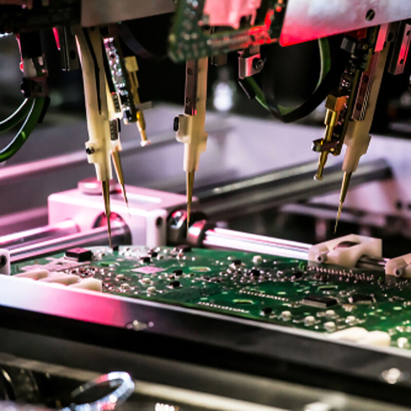
Integriamo sistemi di rilevamento difetti di livello mondiale in ogni fase del processo:
AOI: Attrezzature AOI all'avanguardia scansionano tutte le schede dopo il posizionamento e la saldatura a riflusso, rilevando in tempo reale difetti di saldatura, errori di polarità dei componenti e problemi superficiali. Questa azione riduce i problemi prima che le schede raggiungano la fase di test elettrici.
ICT: Componenti di verifica robusti e sistemi programmabili convalidano la continuità elettrica, i valori dei componenti e l’integrità attiva/a livello di circuito su ogni rete, rilevando circuiti aperti nascosti o valori errati dei componenti.
Verifica funzionale: Le schede destinate ai mercati ADAS, medico e commerciale vengono sottoposte a test funzionali — simulando ingressi/uscite reali, interazioni con il firmware e scenari limite.
Test cardiovascolare ecologico: Per PCB critici per la sicurezza o critici per la missione, KING FIELD esegue test cardiovascolari di affidabilità su lotti casuali e su prototipi, comprendenti cicli termici, vibrazioni, umidità calda e nebbia salina, al fine di eliminare difetti latenti.
MES e tracciabilità digitale: Ogni scheda è contrassegnata con un numero identificativo speciale. Tracciamo l’intera storia: lotto materiale, ID operatore, profilo di rifusione, risultati delle ispezioni e lotto di spedizione.
Calibrazione e manutenzione preventiva: Gli strumenti vengono calibrati regolarmente secondo piani stabiliti in base ai requisiti. Ciò garantisce che ogni giunzione saldata, ogni misura e ogni verifica siano coerenti e affidabili.
Controllo statistico di processo: I parametri critici del processo vengono monitorati in tempo reale e i segnali di fuori controllo attivano immediatamente valutazioni del processo e azioni correttive.
Nonostante i migliori sforzi, si verificano periodicamente problemi o resi per area. KING FIELD garantisce che ogni caso diventi una risorsa di conoscenza:
Analisi della causa radice: utilizzo di raggi X, sezioni trasversali, microscopia elettronica a scansione (SEM) o valutazioni chimiche per individuare la vera origine del problema — sia essa legata al materiale, alla procedura o al design.
Azione correttiva a ciclo chiuso: tutti i riscontri vengono immediatamente tradotti in istruzioni operative aggiornate, revisioni di progetto e osservazioni ai fornitori su eventuali lacune — con conseguenti riduzioni misurabili di difetti analoghi nei cicli produttivi successivi.
Integrazione dei feedback: i dati provenienti dalla VoC (Voice of the Customer) e dai reclami in garanzia vengono reinseriti nelle fasi di progettazione e produzione, favorendo un rapporto di miglioramento continuo con ogni cliente.
KING FIELD è pienamente certificata secondo le norme ISO 9001, IATF 16949 e ISO 13485, nonché certificata IPC-A-600 / IPC-A-610.
Ciò fornisce ai clienti documentazione, trasparenza e garanzia sia sul processo produttivo sia sul prodotto finito.
 Ultime notizie
2026-04-18
2026-04-17
2026-04-13
2026-04-12
2026-04-11
2026-04-10
2026-04-09
2026-04-06