Transform Your Schematic Diagram to PCB Layout with Precision
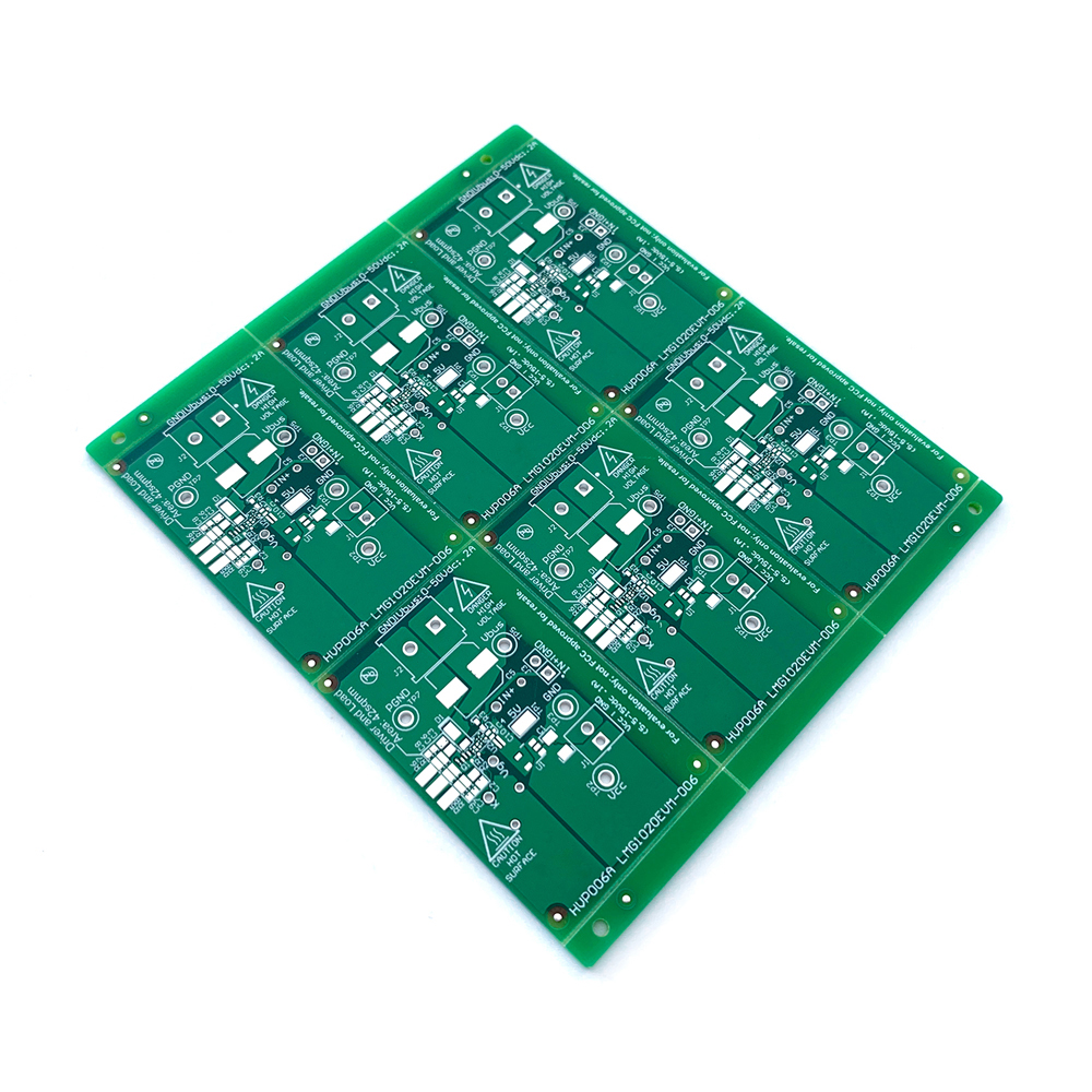
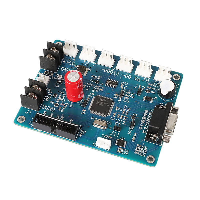
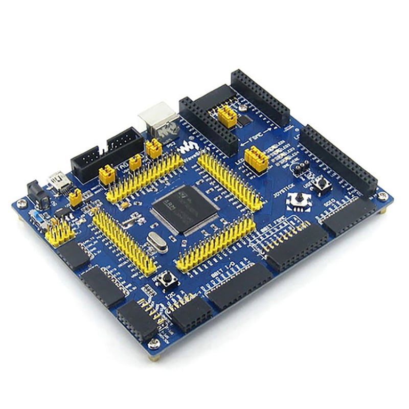
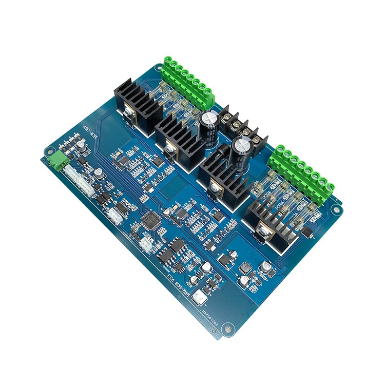
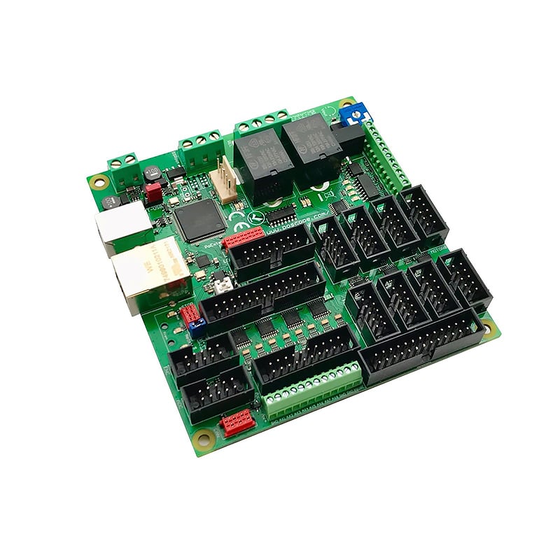
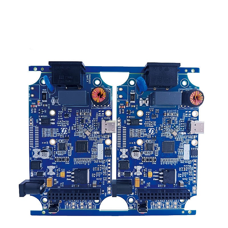
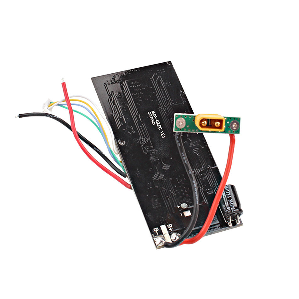
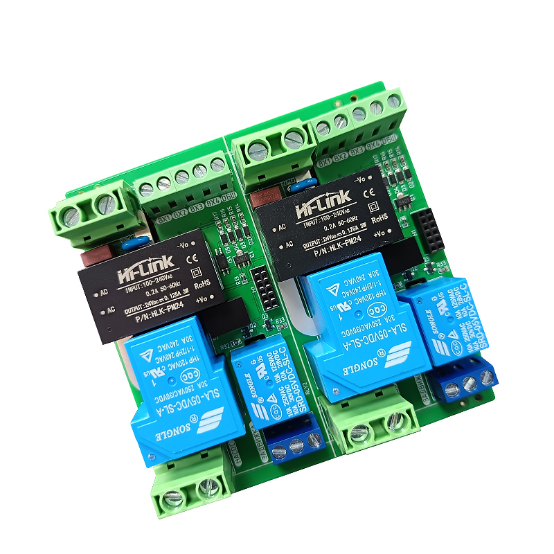
In the realm of electronic design, the transition from a schematic diagram to a PCB layout is a critical step that defines the functionality and efficiency of your electronic product. Our one-stop electronic design and manufacturing service specializes in this intricate process, ensuring that your design is not only accurate but also optimized for performance. With our advanced technology and skilled team, we provide comprehensive solutions that encompass prototype PCB assembly, R&D design, and turnkey PCB assembly services. This includes everything from PCB manufacturing to component sourcing, testing, and final assembly. By focusing on high standards and rigorous quality control, we ensure that your PCB layout meets the demands of various high-end manufacturing fields such as industrial control, automotive, and medical applications. Partner with us to transform your schematic diagrams into high-quality PCB layouts that drive innovation and efficiency in your products.
Get A Quote

 EN
EN