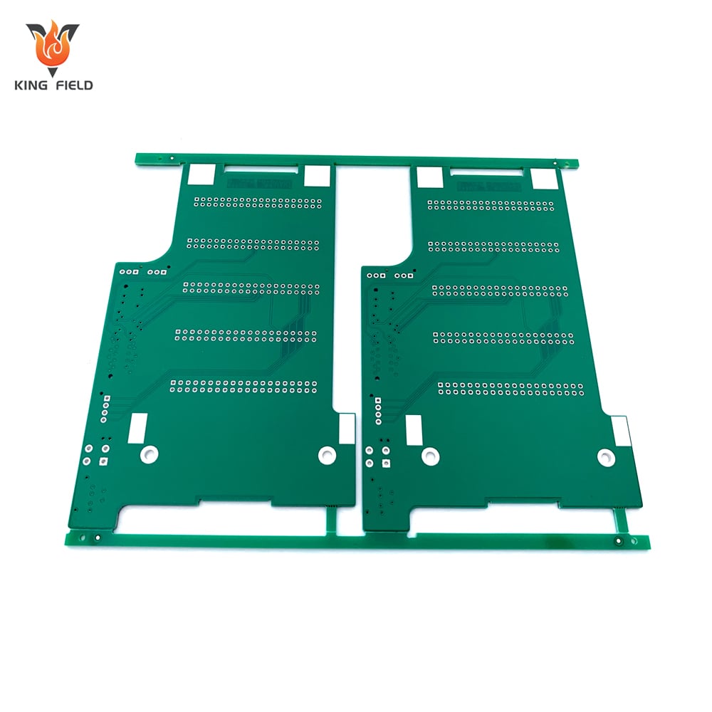
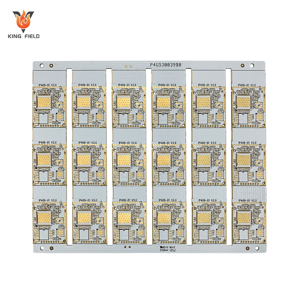
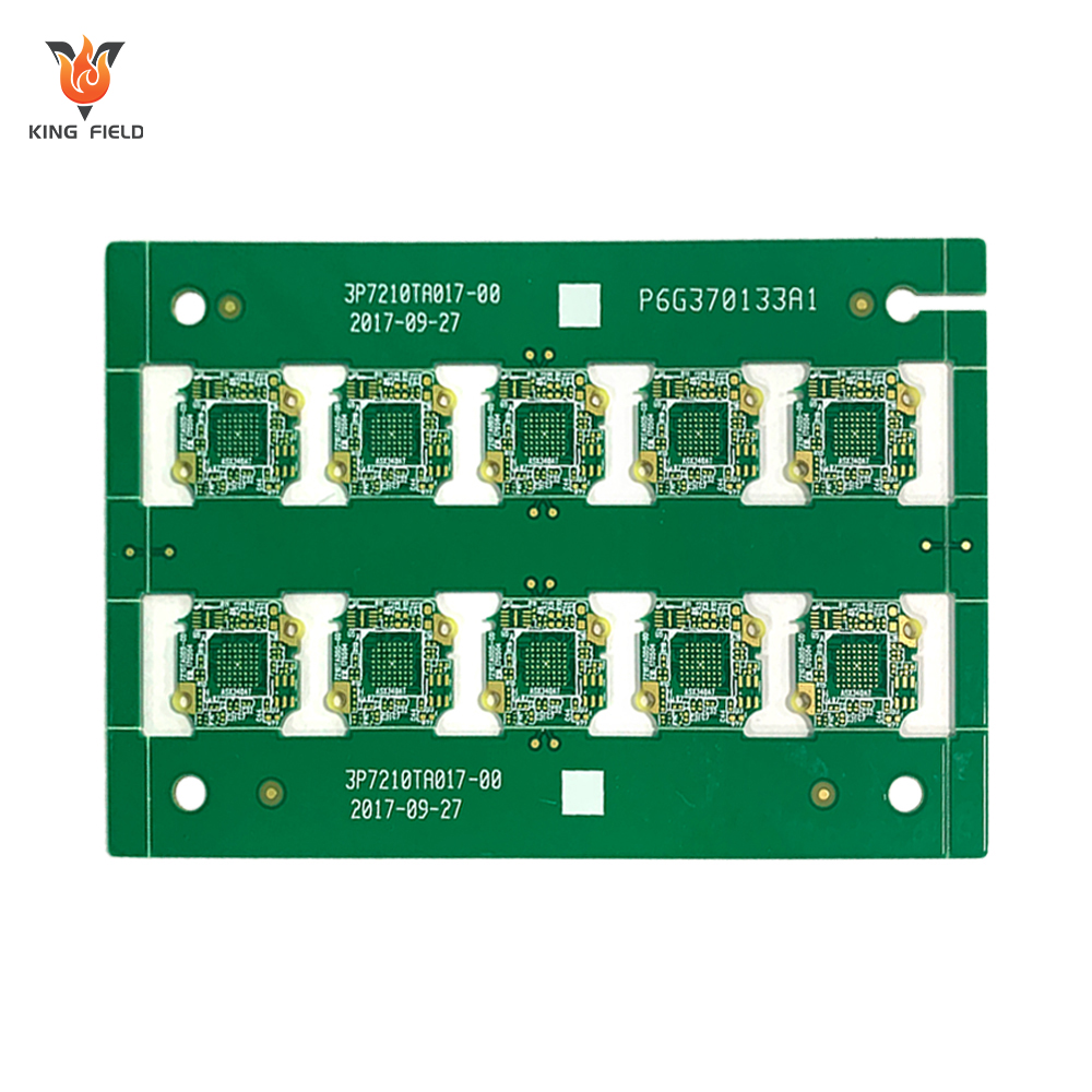
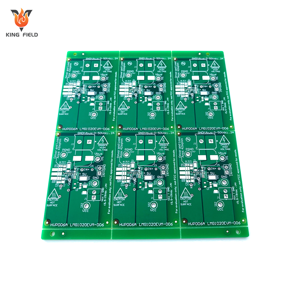
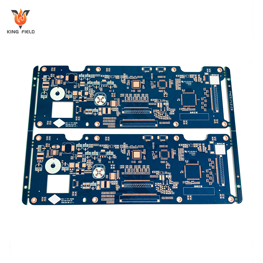
Rigid PCBs
KING FIELD has over 20 years of industry experience in PCB prototyping and manufacturing . We pride ourselves on being your best business partner and close friend, meeting all your PCB needs.
☑ 20+ years of PCB manufacturing experience
☑Supports blind vias and micro vias
☑ The solder mask tolerance is 0.025mm.
Description
- Number of floors: 1-40
- Surface treatments: Electroless nickel immersion gold (ENIG) , electroless nickel immersion gold (ENEPIG) , immersion tin , hot air leveling (HASL) , immersion silver , lead-free hot air leveling (Lead-free HASL) , electrolytic bonding with wire bonding.
- Minimum trace spacing: 0.051 mm
- Solder mask characteristic tolerance: 0.025 mm
- 35:1 borehole aspect ratio
- Maximum panel size: 24 inches × 30 inches (approximately 60.96 cm × 76.2 cm)
- Blind vias and micro vias
- Through-pad (supports conductive fill, non-conductive fill, copper plug fill, and other options)
- Support blind buried holes
- Fast delivery
What is a rigid PCB?
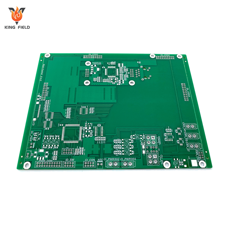
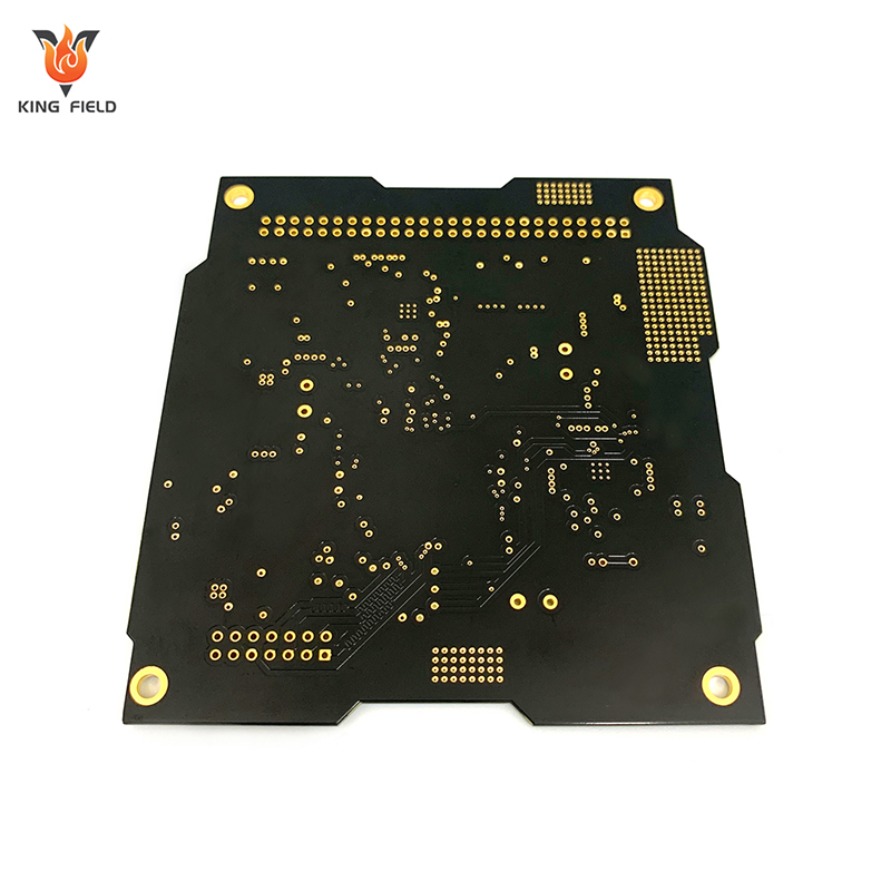
Rigid pcb board are traditional non-flexible circuit boards made of solid substrates. The most commonly used substrate is FR4 (glass fiber epoxy resin laminate), which provides mechanical stability for circuits and components.
KING FIELD's rigid PCB manufacturing capabilities
Project |
Ability |
Outer layer traces/spacing |
0.002 inches / 0.002 inches (approximately 0.005 millimeters / 0.005 millimeters) |
Inner layer routing/spacing |
0.002 inches / 0.002 inches (approximately 0.005 millimeters / 0.005 millimeters) |
Minimum borehole diameter |
0.002 inches (approximately 0.005 millimeters) |
Standard borehole diameter |
0.008 inches (approximately 0.020 millimeters) |
Drilling aspect ratio |
35:1 |
Minimum pad size |
0.004 inches (approximately 0.010 millimeters) |
Minimum feature distance to plate edge |
0.010 inches (approximately 0.025 millimeters) |
Minimum core board thickness |
0.001 inches (approximately 0.0025 millimeters) |
Why choose KING FIELD as your rigid PCB manufacturer?
As a manufacturer of rigid-flex printed circuit boards, KING FIELD serves the global market, providing both all-inclusive and customer-supplied-materials rigid circuit board manufacturing services.
- One-stop engineering support from design to mass production
KING FIELD is committed to providing one-stop PCB /PCBA electronic design and manufacturing services . Our services are a manufacturing platform that integrates front-end R&D design, component procurement, precision SMT placement, DIP insertion, complete assembly, and full-function testing.
- 20+ years of craftsmanship accumulation
- Our core team members have an average of 20+ years of experience with Rigid Flex . Practical PCB experience, covering circuit design, process development, production management, and other fields.
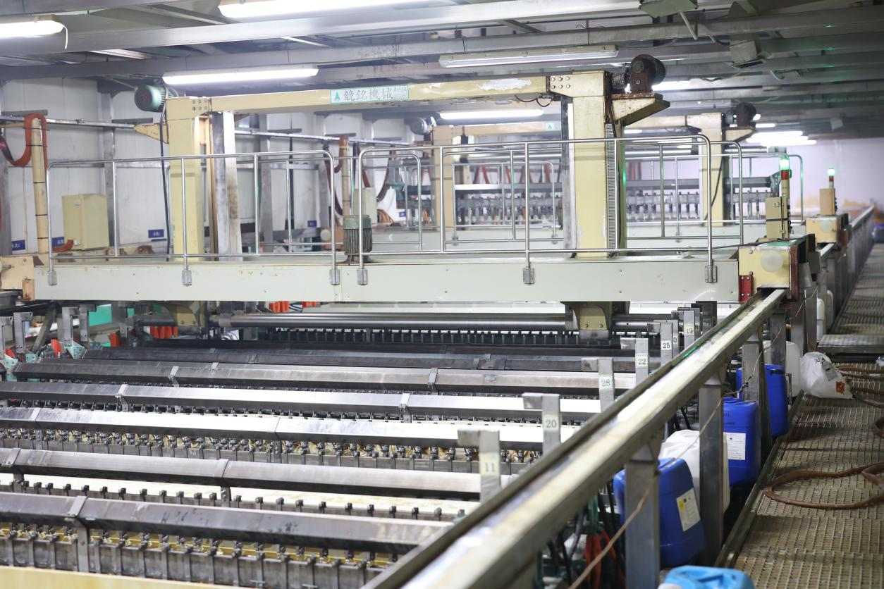
- Currently, it has a research and development team of 50+ people and a front-line production team of 600+ people , with a modern factory area of 15,000+ square meters.
l Transportation support
Domestic shipping is handled by SF Express/Deppon Logistics, with full coverage; international shipping is also available via DHL/UPS/FedEx, with professional shockproof packaging ; and triple protective packaging including anti-static, anti-oxidation, and anti-collision protection.

FAQ
Q1 : How do you avoid delamination and bubbles during the lamination process of multilayer boards?
KING FIELD: We use prepreg vacuum packaging, and allow it to warm up for 24 hours before use ; then we use ultrasonic scanning to detect voids, and finally we periodically slice and analyze the bonding state between the layers to ensure it is good .
Q2 : How do you control the linewidth and dielectric thickness ?
KING FIELD: We perform side etching compensation based on the copper thickness during the design phase , then use LDI laser direct imaging to avoid deformation, and finally verify the thickness of each dielectric layer through slicing analysis and laser thickness gauge .
Q3 : How do you solve the problem of electroplating uniformity in deep holes with high aspect ratio?
KING FIELD: We use pulse electroplating technology, combined with plasma cleaning, to remove drilling contaminants inside the holes and make the roughness uniform.
Q4 : How do you avoid adhesion problems and appearance defects in solder resist ink?
KING FIELD: We use chemical cleaning and mechanical abrasion, combined with plasma activation treatment, to control the surface roughness to Ra 0.4-0.6μm , and then perform high-precision screen printing: screen tension 25-30N/cm, squeegee angle 60° . Finally, we conduct adhesion tests: 3M tape showed no peeling .
Q5 : How do you control the warping and deformation of large-size boards?
KING FIELD: We use symmetrical lamination for optimization to reduce internal stress , and then use vacuum pressing to control the heating rate at an appropriate level , and then apply pressure in stages .