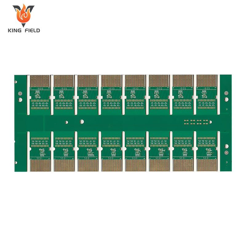
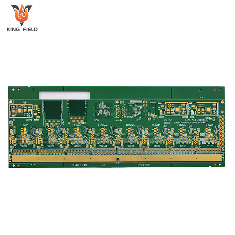
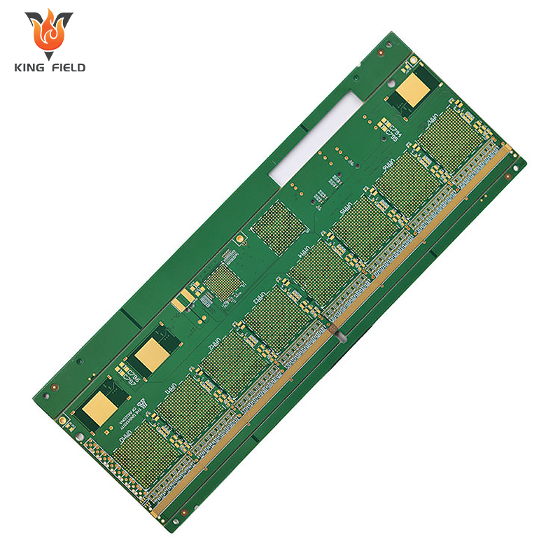
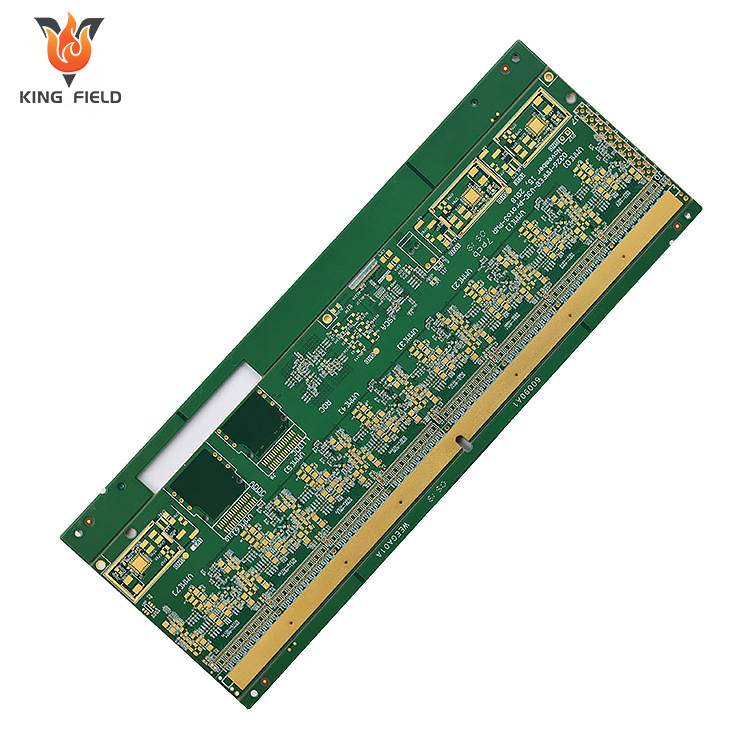
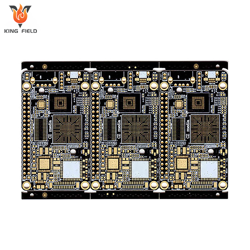
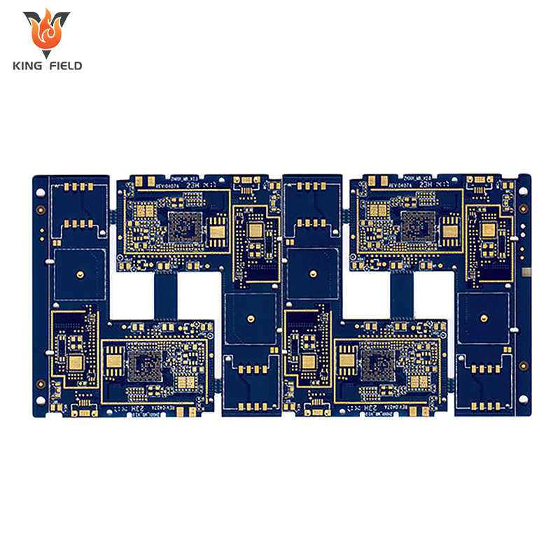
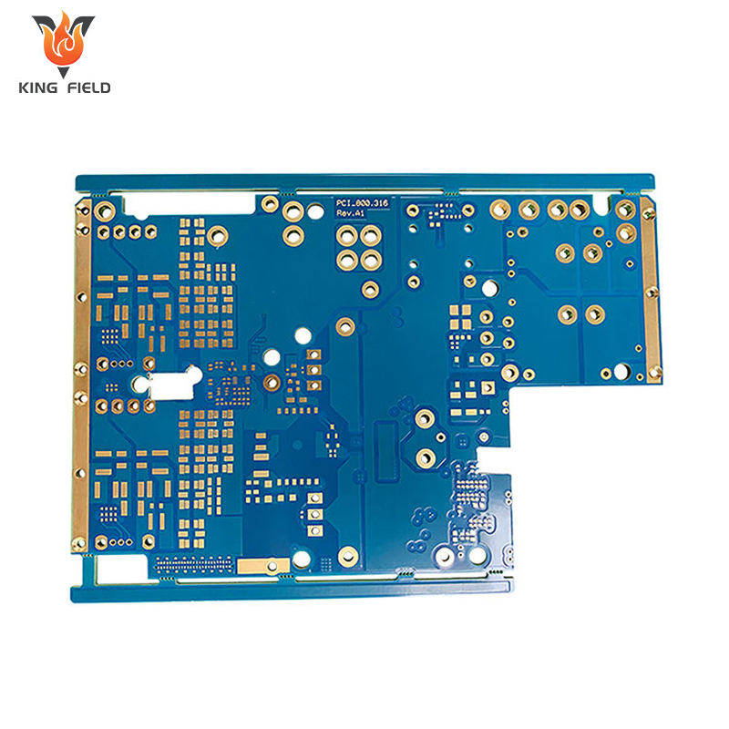
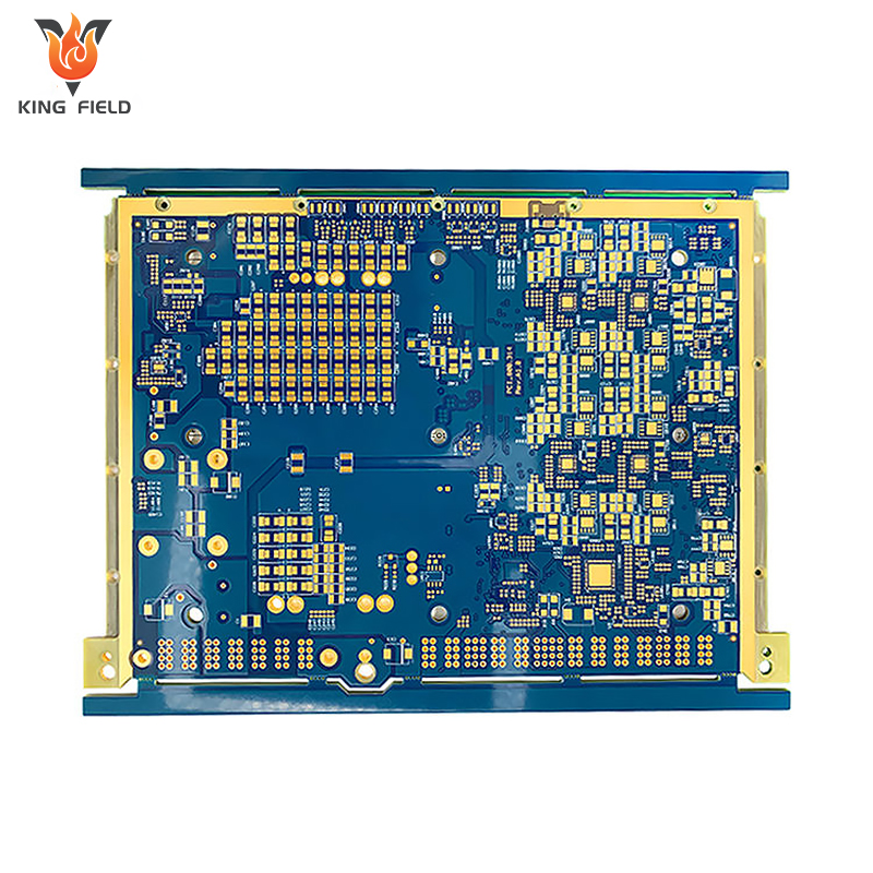
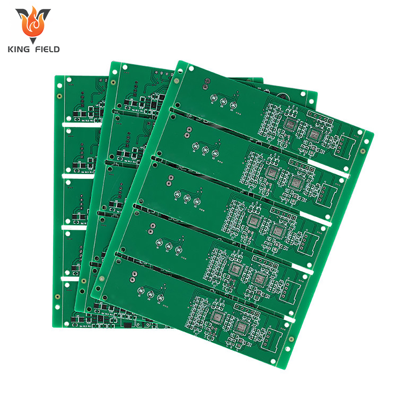
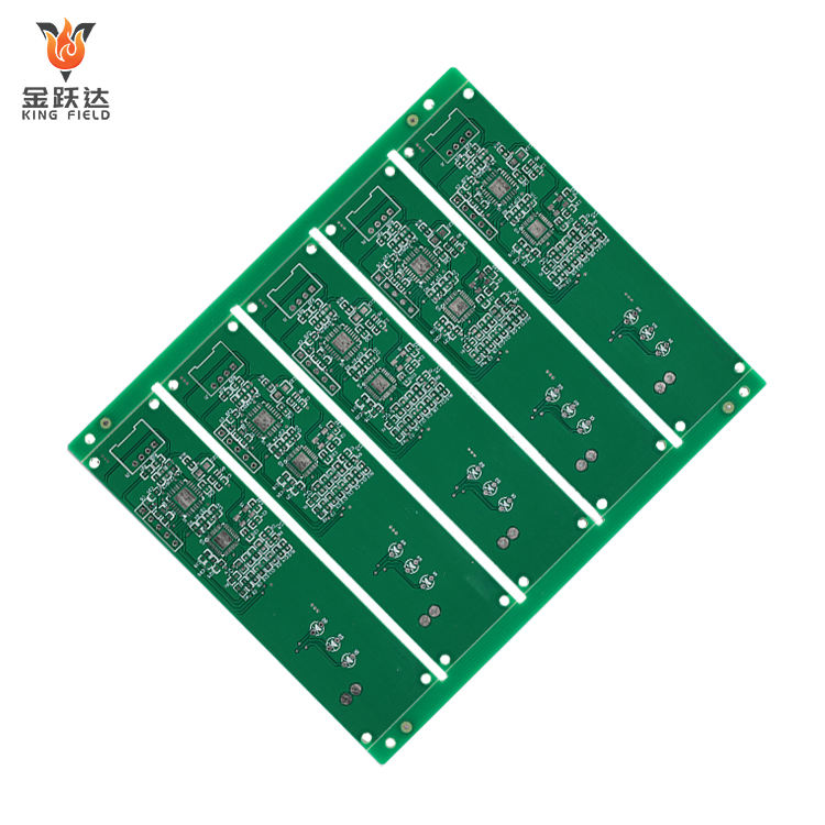
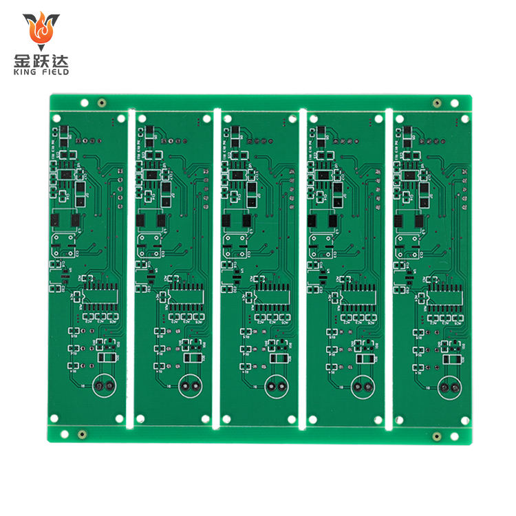
HDI PCB
As one of the world's leading PCB manufacturers, KING FIELD always treats its customers as partners, aiming to become their most reliable business collaborator. Regardless of project size, we guarantee a 99% on-time delivery rate. From prototyping to mass production, we will support every PCB need of yours with professionalism and sincerity.
☑ Employs fine-pitch traces, microvias, and a space-saving design.
□ Rapid delivery, DFM support, and rigorous testing.
☑ Improve signal integrity and reduce size.
Description
Via Types:
Blind via, buried via, through-hole via
Number of layers:
Up to 60 layers
Minimum line width/line spacing:
3/3mil (1.0OZ)
PCB board thickness:
0.8-3.2mm, 0.1-8.0mm (evaluation required for less than 0.2mm or greater than 6.5mm)
Minimum mechanical aperture:
0.15mm (1.0OZ)
Minimum laser aperture:
0.075-0.15mm
Surface treatment type:
Immersion gold, immersion nickel palladium gold, immersion silver, immersion tin, OSP, spray tin, electroplating gold
Board type:
FR-4, Rogers series, M4, M6, M7, T2, T3
Application areas:
Mobile communications, computers, automotive electronics, medical
PROCESS CAPABILITIES
ITE project |
model |
batch |
number of floors |
4-24 Layers |
4-16 Layers |
Laser process |
CO2 Laser Machine |
CO2 Laser Machine |
TG value |
170°C |
170°C |
Kong Tong |
12-18µm |
12-18µm |
Impedance tolerance |
+/- 7% |
+/- 10% |
Interlayer alignment |
+/-2mil |
+/- 3mil |
solder mask alignment |
+/- 1mil |
+/-2mil |
Medium thickness (Min) |
2.0mil |
3.0mil |
Pad size (Min) |
10mil |
12mil |
Blind aperture aspect ratio |
1.2:1 |
1:1 |
Line width/line spacing (Min) |
2.5/2.5mil |
2.5/2.5mil |
Hole ring size (Min) |
2.5mil |
2.5mil |
Through-hole diameter (Min) |
6mil (0.15mm) |
8mil (0.2mm) |
Blind hole diameter (Min) |
3.0mil |
4.0mil |
Plate thickness range |
0.4-6.0mm |
0.6-3.2mm |
Order (Max) |
Any layer interconnected |
4+N+4 |
Laser aperture, (Min) |
3Mil (0.075mm) |
4mil (0.1mm) |
KING FIELD : A Reliable HDI PCB Manufacturer in China
KING FIELD for HDI PCB :
Founded in 2017, Shenzhen Jinyueda Electronics Co., Ltd. is based in Bao'an District, Shenzhen, and has a professional team of more than 300 people.
As a high-tech enterprise specializing in one-stop electronic design and manufacturing, we have built a complete manufacturing platform integrating front-end R&D design, procurement of superior components, precision SMT placement, DIP insertion, complete assembly, and full-function testing. Our team members have an average of over 20 years of practical experience in the PCB industry . Choose KING FIELD for your HDI PCB needs to help you launch your products.
- Supports multiple HDI structures
1+N+1
, 2+N+2
, 3+N+3 and multi-stage HDI (suitable for high-end intelligent devices)
- Fast delivery
KING FIELD's standard HDI samples can be shipped within 6 days, suitable for R&D and small-batch production.
Professional engineers optimize production processes, lead times, and improve yield rates.
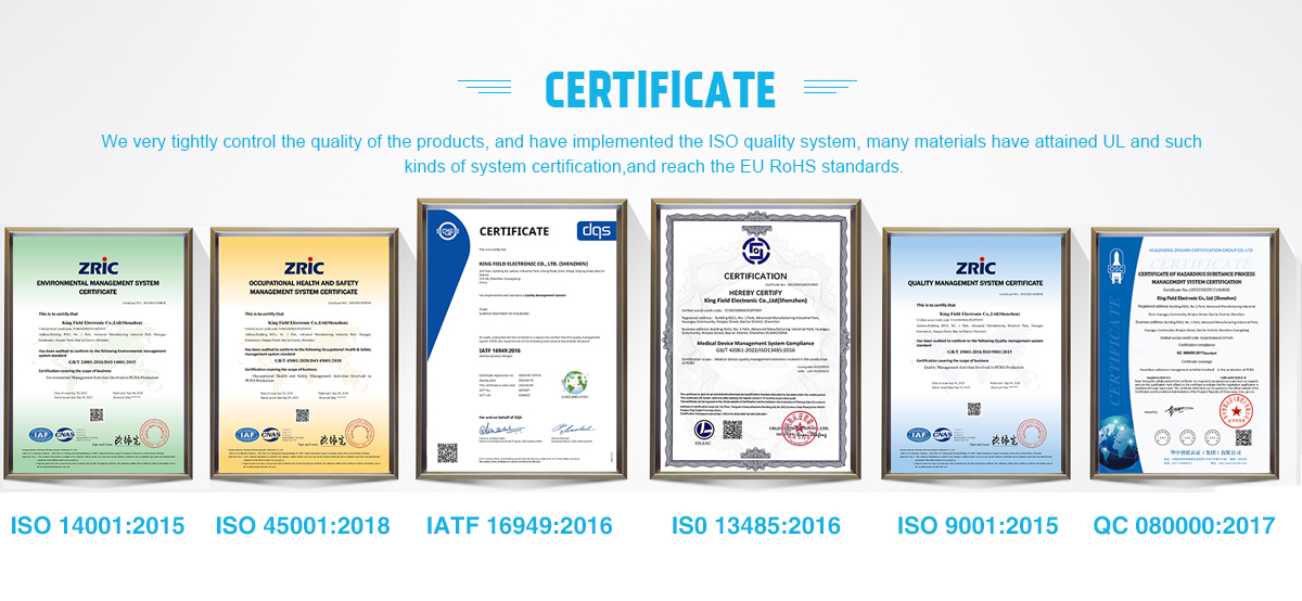
- Quality Assurance and Certification
We are ISO9001 and UL certified, and comply with IPC standards. Our PCBs
undergo rigorous electrical and reliability testing to ensure long-term stability.
- Advanced materials and surface treatment
We provide high -TG materials (≥170℃), suitable for high-temperature environments such as 5G and automotive electronics.
They support various surface treatments such as immersion gold and nickel-palladium-gold plating to improve welding reliability.
- High-precision manufacturing capabilities
Laser beam technology supports the fabrication of micro-blind vias.
The minimum line width/spacing can reach 3mil, meeting the needs of high-density wiring.
Comprehensive after-sales support system
KING FIELD offers an industry-uncommon "1-year warranty + lifetime technical support" service. We promise that if a product has a non-human-caused quality problem, it can be returned or exchanged free of charge, and we will bear the relevant logistics costs.
Our shipping method
KING FIELD offers efficient and reliable international shipping services, safely delivering your orders to over 200 countries and regions worldwide. We promise that all packages are fully trackable, and you can check the real-time logistics status on your order page at any time .

FAQ
Q1: How to ensure the processing quality and reliability of microvias (blind/buried vias)?
KING FIELD: We employ stepped laser drilling, adjusting pulse energy and focal length for different dielectric layers; we use plasma cleaning or chemical desmearing to treat the hole walls, enhancing the adhesion of the chemical copper; for blind holes, we use electroplating filling technology, coupled with a specialized filling electroplating solution.
Q2: How can we effectively control the alignment accuracy between multiple layers ?
KING FIELD : We use highly stable materials and conduct 24-hour temperature and humidity balancing before production ; combined with a CCD optical alignment system and an optimized stepped pressing process, we solve the problems of reducing resin flow rate and uneven pressure .
Q3: How to achieve high-precision fabrication of fine circuits?
K ING FIELD: Of course, it uses LDI laser direct imaging to replace traditional exposure, with an accuracy of ±2μm; and it uses horizontal pulse etching or semi-additive process to solve the problem of improper control of etching solution.
Q4: How to ensure the uniformity of the dielectric layer thickness to meet impedance requirements?
KING FIELD: We will select low-flow PP material and conduct multi-layer pre-stack testing; then use vacuum pressing technology and perform 100% thickness testing on key layers, and compensate for deviations by adjusting the PP combination.
Q5: How to solve the problem of electroplating uniformity and adhesion of micropores with high aspect ratio?
KING FIELD: King Field uses pulse electroplating technology, combined with vibrating anodes, to improve the uniformity of copper plating in deep holes; then it establishes an online monitoring system for the chemical solution to adjust the copper ion concentration and additive ratio in real time; and it performs secondary copper plating on special holes to solve the problems of uneven copper plating/poor adhesion.