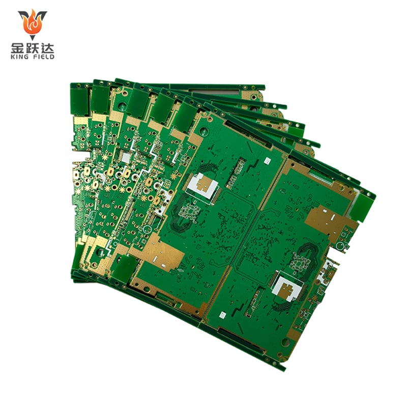
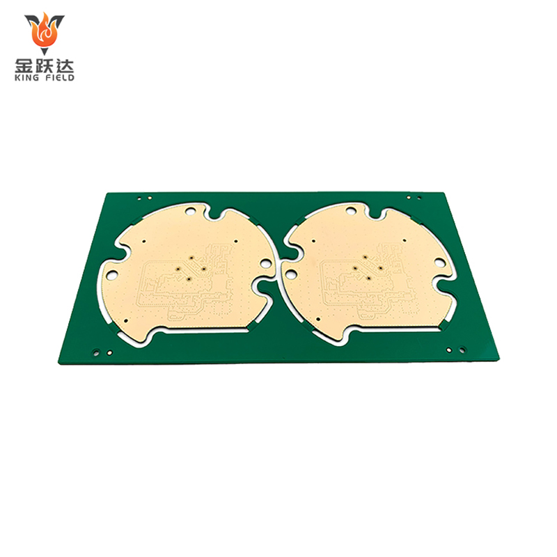
Multilayer PCB
KING FIELD has over 20 years of industry experience in PCB prototyping and manufacturing. We are committed to providing our customers with one-stop PCB/PCBA solutions .
☑ 20+ years of PCB industry experience
☑ Rush orders delivered within 24 hours
☑Finished copper thickness: 1-13 ounces
Description
Multilayer PCB
Substrate: FR4
Number of floors: 4
Dielectric constant: 4.2
Plate thickness: 1.6mm
Outer copper foil thickness: 1oz
Inner copper foil thickness: 1 oz
Surface treatment method: Immersion gold
What is a multi layer pcbs?
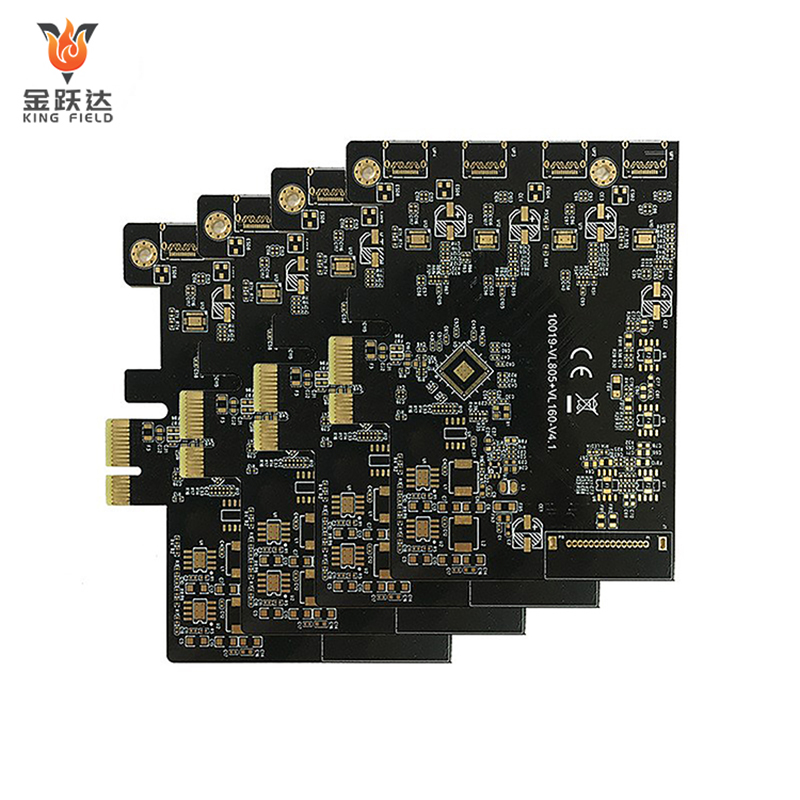
Multilayer PCBs are printed circuit boards with more than two copper layers. In contrast, single-layer and double-layer PCBs have only one or two copper layers. Multilayer circuit board typically have 4-18 layers, and in special applications, they can even have up to 100 layers.
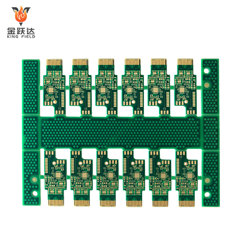
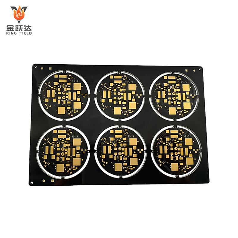
KING FIELD's multilayer PCB manufacturing capabilities
Project |
Ability |
Substrate: |
FR-4, high Tg FR-4, Rogers materials, polytetrafluoroethylene (PTFE), polyimide, aluminum substrate, etc. |
Dielectric constant: |
4.2 |
Outer copper foil thickness: |
1oz |
Surface treatment method: |
Lead-based hot air leveling (HASL), lead-free hot air leveling (HASL), chemical immersion gold, organic solder mask (OSP), hard gold |
Minimum line width: |
0.076 mm / 3 mils |
Finished copper thickness |
1-13 ounces |
Solder mask color |
White, Black |
Testing methods |
Flying probe testing (free), Automated Optical Inspection (AOI) |
Copper thickness: |
1 ounce - 3 ounces |
Shelves: |
4 floors |
Plate thickness: |
0.2-7.0 mm |
Inner copper foil thickness: |
1oz |
Minimum aperture: |
Mechanical drilling: 0.15 mm; Laser drilling: 0.1 mm |
Minimum line spacing: |
0.076 mm / 3 mils |
Impedance requirements: |
L1, L350 ohms |
Delivery cycle |
24 hours |
Why choose KING FIELD as your multilayer PCB manufacturer?
20+ years of experience in multilayer PCB manufacturing
- Since 2017 , KING FIELD, a high-tech enterprise focusing on one-stop PCBA manufacturing, has always been committed to "creating an industry benchmark for ODM/OEM PCBA intelligent manufacturing" and has steadily cultivated the high-end manufacturing field.
- Currently, we have a research and development team of 50+ people and a front-line production team of 600+ people.
- Our core team members have an average of 20+ years of practical experience in PCB/ PCBA, covering areas such as circuit design, process development, and production management .
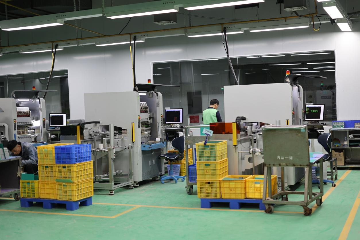
Fully equipped
KING FIELD's multilayer PCB production and testing equipment mainly includes: laser drilling, LDI exposure machine, vacuum etching machine, laser forming, multilayer board hot press, online AOI optical inspection, four-wire (low resistance) tester, and vacuum resin plugging.
A sound quality control system
- Made with lead-free, halogen-free and other environmentally friendly materials, all products undergo multiple tests, including AOI optical scanning, flying probe testing, and (four-wire) low resistance testing.
- In terms of quality control , KING FIELD has passed six major system certifications: IATF 16949, ISO 13485, ISO 9001, ISO 14001, ISO 45001, and QC 080000. We also have 7 SPI, 7 AOI, and 1 X-Ray testing equipment to ensure quality throughout the process. Our MES system enables full traceability of every PCB/PCBA product .
Production capacity
- We own an SMT assembly plant with a total area of over 15,000 square meters, which can realize integrated production of the entire process from SMT placement and THT insertion to complete machine assembly.
- KING FIELD's production line is equipped with 7 SMT lines, 3 DIP lines, 2 assembly lines, and 1 painting line. Our YSM20R placement accuracy can reach ±0.035mm, and it can handle components as small as 0.1005mm . The daily production capacity of SMT is 60 million points; the daily production capacity of DIP is 1.5 million points.
Minimum order quantity for multilayer PCBs
delivery time from prototyping to mass production of multilayer PCBs :
Prototype production: 24-72 hours ; <50 pieces : 3-5 working days ; 50-500 pieces : 5-7 working days ; 500-1000 pieces: 10 working days; >1000 pieces: according to the bill of materials.
Transportation support
Domestic shipping is handled by SF Express/Deppon Logistics, with full coverage; international shipping is also available via DHL/UPS/FedEx, with professional shockproof packaging ; and triple protective packaging including anti-static, anti-oxidation, and anti-collision protection.
FAQ
Q1 : What is the thickness tolerance you can control for your multilayer PCB boards?
KING FIELD: Our board thickness tolerance can be controlled within ±0.08mm (1.0-2.0mm board thickness) .
Q2 : What is the maximum aspect ratio (thickness-to-diameter ratio) of your multilayer boards ?
KING FIELD: Our mass production capacity range is: board thickness 2.0mm, hole diameter 0.2mm, aspect ratio 10:1.
Q3 : How do you control the drilling quality of multilayer boards?
KING FIELD: We first drill the guide holes with a small drill bit, and then enlarge the holes to the final size with a standard drill bit. For critical signal holes, we use laser drilling, combined with post-processing methods such as plasma cleaning , to ensure drilling quality.
Q4 : How do you ensure the reliability of high-density interconnects (HDI)?
KING FIELD: We use UV laser drilling to control the hole diameter to 0.05-0.15mm and maintain the positional accuracy to ±10μm . Then we use plasma for chemical cleaning, mainly to control the micro-hole fabrication and dielectric layer.
Q5 : How is impedance control achieved in multilayer boards?
KING FIELD: We use HFSS/CST software to consider actual material parameters, preset line width /spacing compensation values based on historical data , and then use TDR testing to control the difference within ±5% , thus achieving high consistency control of multilayer board impedance through multiple methods.