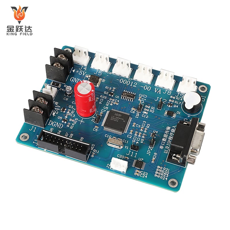
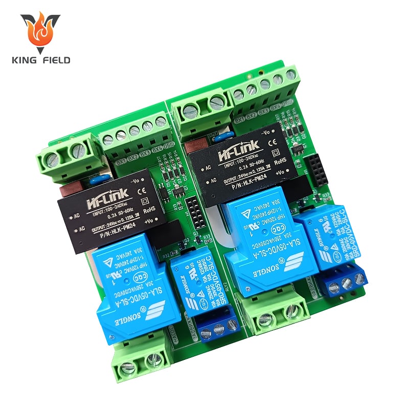
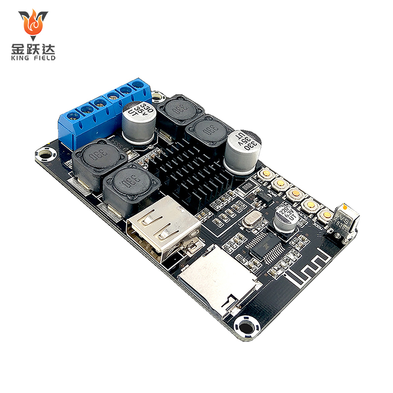
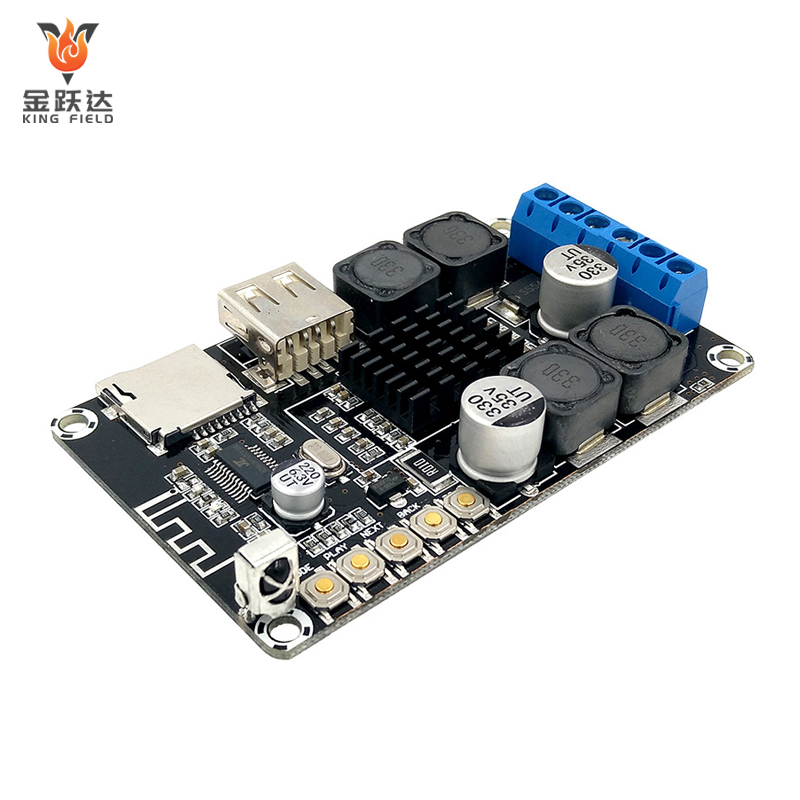
PCB Design & Layout
KING FIELD is a PCBA manufacturer with over 20 years of professional manufacturing experience. We are committed to providing customers with one-stop PCB /PCBA solutions.
☑ We support ODM/OEM.
☑One -stop PCB/PCBA manufacturing experience
☑ 20 years of PCBA solution development experience
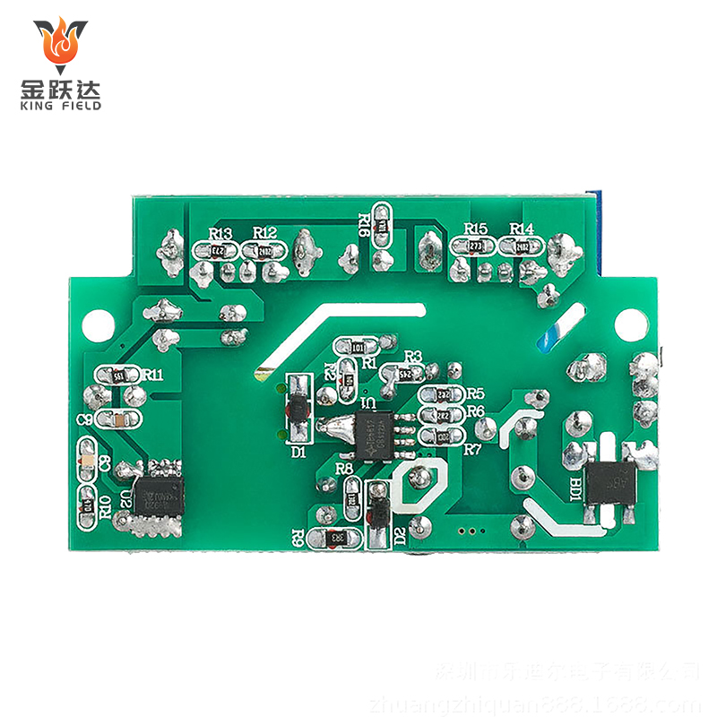
Description
KING FIELD 's PCB layout design Advantages
Founded in 2017, KING FIELD has been focusing on designing printed circuit boards (PCB), production of PCB lines, sourcing of components, SMT assembly, and testing of products. We aim to provide customers with comprehensive PCB/PCBA solutions.
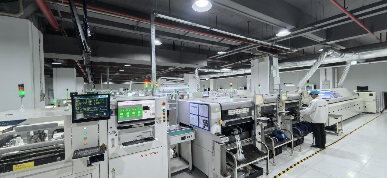
We have very modern machinery
We have 5 fully automated surface mount technology (SMT) production linesCryogenic reflow solderingWave solderingFull automatic conformal coating machine
Fully automatic solder paste printing machine
3D AOI and X-ray inspection equipment
Selective wave soldering
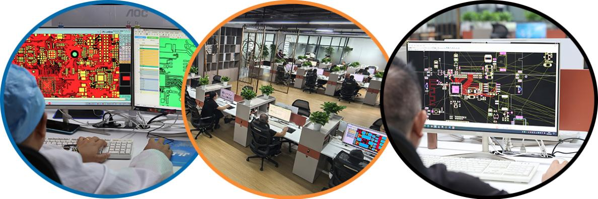
Well-trained design team
Our design engineers boast 20 years of experience in creating PCB/PCBA solutions. Besides being proficient in circuit design and layout, they also possess knowledge of best manufacturing practices.
Besides that, they are familiar with numerous widely used design software packages.
Furthermore, since we do all the work ourselves, we can arrange the job so that the production can start right after the design is done, and this will save you a lot of time. KING FIELD' production area is fitted with 7 SMT lines, 3 DIP lines, 2 assembly lines, and 1 coating line.
We possess a YSM20R with a placement accuracy of ±0.015mm that is capable of handling very small components down to 0.1005.
Our maximum daily SMT input is 60 million points, and our maximum daily DIP input is 1.5 million points.
Turnkey service
Being a one-stop shop, we provide the whole manufacturing platform which integrates R&D, design at the frontend, procurement of wonderful components, very accurate SMT placement, DIP insertion, complete product assembly, and fully functional testing.
Quick development and delivery
With the support of our efficient design team, the development of PCB can be accomplished in the shortest period of time. Occasionally, we are able to turnover your requests within 24 hours.
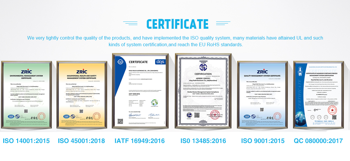
Quality Assurance
KING FIELD's PCB design excellence is ensured by our MES system that permits complete traceability of the production process for each PCB/PCBA. In addition, our company has acquired ISO13485, ISO9001, IATF16949, ISO14001 and ISO45001 certification.
Manufacturing strengths
Having our own SMT assembly line allows us to operate with great flexibility, optimize how we utilize our resources and get the best from our operating expenses, all of which in turn lead to our precise control of cost, quality and delivery time.
FAQ
Q1: What measures do you take to make sure that high-speed signal transmission is free from errors?
KING FIELD: Matching impedance accurately, wiring strictly, and using a proper line spacing and layer isolation are the main ways we limit the signal reflection and even eliminate errors in high-speed data transmission.
Q2: What measures do you take to guarantee that your PCB designs can successfully pass the CE/FCC certification?
KING FIELD: We first design the layers so that the high-speed signals are always running very close to the ground plane, thus limiting the radiation. Then, we place the filter elements on the interfaces and sensitive circuits, which block the interference sources. Finally, we modify the ground design such that there is no loop antenna formation, thus facilitating the passing of the certification at the very first attempt.
Q3: How do you solve the heat dissipation problem of high-power devices?
KING FIELD: The design includes a very tightly packed cluster of high-temperature vias under the heating elements. Also, copper paths that carry current are made wider and components that are very sensitive to heat are placed far away from the areas where it's hot.
Q4: What do you do to prevent production issues such as soldering defects from occurring?
KING FIELD: We do not only prevent surface mount defects by optimizing the design of pad sizes and solder mask openings but also verify that the spacing between components corresponds to the clear alignment requirements of the PICK & PLACE machine's MARK points.
Q5: How do you make sure that the PCBs can be assembled accurately?
KING FIELD: 3D structural support is a feature of our collaborative design. After your shell model will be uploaded, we carry out real-time layout and collision-free checks to ensure that connectors, buttons, and screw holes are perfectly matched with the shell openings.