PCB Layout
As a PCBA manufacturer with over 20 years of professional experience , KING FIELD is committed to providing customers with one-stop PCB/PCBA solutions.
☑Minimum BGA pin pitch is 0.3mm
☑ Sign a confidentiality agreement
☑ Multilayer/HDI/Fine Pitch Packaging Technology
Description
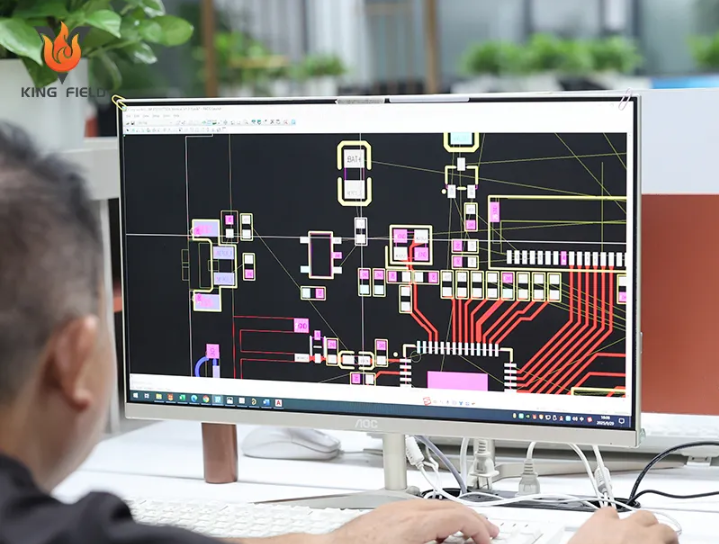
What is PCB layout?
Simply put, PCB layout is the complex and essential art of deciding where the components, copper traces, soldering pads, vias, and so on, should be physically placed on the printed circuit board according to the circuit diagram.
Advantages of Using KING FIELD’s PCB Layout Service
Highly Skilled Engineering Team
We are blessed with a professional PCB layout design team which has been actively designing product layouts for over 20 years and is proficient in designing various types of high-layer, high-speed, and high-density products.
Counting 2000 product designs delivered every year, our team has earned an excellent reputation amongst over 1000 clients and has successfully completed numerous projects.
Advanced and excellent quality assurance system
Self-check system: Each design stage is carefully checked using detailed checklists.
Expert Review: The design scheme, production feasibility, testability, EMC, and thermal performance of a product are assessed by the senior experts.
We are fully capable of opposing EMC, SI, reliability designs, and using our developed DFM software for performing production feasibility checks.
Fast assembly service
By doing parallel designing, the delivery cycle is reduced by 30%-50%
Internal manufacturing: Processes can be executed immediately without any additional waiting time.
High confidentiality
We sign a confidentiality agreement for every order, and our designers' computers are fully encrypted to make sure our clients' files remain 100% confidential.
Self-check
A thorough quality system, and self-inspection mechanism, including a checklist for layout, wiring, regularity, beauty, and thermal design.
Expert review
Senior team members of KING FIELD will attend the review, checking the aspects of schematic design, DFM, DFT, high speed, EMC, and thermal design comprehensively.
KING FIELD PCB Layout Work Flow
Place layout order online → Get quote assessment → Confirm prepayment → Start working → Confirm layout → Perform overall review → Complete project → Make final payment
Up to 100 floors |
40 floors |
BGA pitch |
≥0.2mm |
Minimum line width |
2.4mil |
Minimum line spacing |
2.4mil |
Highest speed signal |
60GHz |
Maximum number of connections |
78000+ |
BGA-PIN number |
≤2500 |
FAQ
Q1 Are your boards difficult to manufacture?
KING FIELD: It should not be a problem if the process is well defined: We will check the board process capability before we do the design, workmanship to make sure line width and hole diameter; while routing, we will also make sure that the distance from the drill hole to copper, solder mask bridges, and characters not pressing on solder pads are all well kept.
Q2. Is the power supply of your board stable?
KING FIELD: We first enlarge high current track and then add vias to share the current . Putting small capacitors near the power pins of each chip has also been done by us as well as adding heat dissipation vias to the bottom of the power devices to prevent local overheating and guarantee uninterrupted power supply.
Q3. Can your high-speed signal operate stably?
KING FIELD: Our process will include impedance calculation, asking for test reports after board deployment , and keeping the length error of parallel bus data lines such as DDR within ±50mil ; besides, sensitive signals should be kept away from interference sources and grounded to avoid crossing splits .
Q4. Are the boards you design certified and radiation-free?
KING FIELD: At the very least, we carefully isolate the digital/analog/power zones, then place protective devices at the interfaces, and run high-speed signals along the ground plane to reduce the loop area.
Q5. Are your boards easy to test and repair?
KING FIELD: We always include a test point with a diameter of ≥1mm , and operating space is reserved around the reference designators of large components , as well as around the reference designators of critical components .