PCB Stencil
KING FIELD has over 20 years of industry experience in PCB prototyping and manufacturing . We pride ourselves on being your best business partner and close friend, meeting all your PCB needs.
☑ The stencil openings are precise, with an accuracy of ±20µm.
☑ Made with imported Japanese 304 stainless steel spring sheets
☑ High hardness, high temperature resistance, easy to clean
Description
What is a PCB stencil?
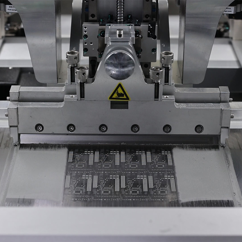
A PCB stencil is a thin piece of material which has openings at spots that coincide with the solder pads of the PCB. It precisely allows the application of solder paste only to those parts of the printed circuit board and also includes reference marks that are used for the alignment of the boards during manufacturing. This machine is the backbone of surface-mount technology (SMT) assembly process at which the electronic components are soldered directly on to the PCB surface. Among various techniques, stencil printing is the fastest for deposition of solder paste in high-volume manufacturing.
KING FIELD PCB Stencil
Materials:
Stainless steel, aluminum frame, AB resin adhesive , nickel , polyimide
Steel mesh types:
framed steel mesh , frameless steel mesh , electroformed steel mesh , stepped steel mesh , laser-cut and electropolished steel mesh .
Manufacturing methods:
laser cutting, chemical etching, electroforming
Minimum BGA thickness:
rigid boards 0.3mm; flexible boards 0.4mm;
Minimum precision lead size: 0.2mm
Component assembly accuracy: ±0.015mm
SMT capacity: 60,000,000 chips/day
KING FIELD steel mesh thickness:
KING FIELD provides various stencil thicknesses such as 0.08mm / 0.1mm / 0.12mm / 0.15mm / 0.2mm / 0.3mm. To accommodate the finest-pitch QFP and BGA components as well as the smallest chip components, stencil thickness should ideally be considered during design.
Component type |
spacing |
Steel mesh thickness |
CHIP |
0402 |
0.12mm |
0201 |
0.10mm |
|
BGA |
1.25~1.27 |
0.15mm |
1.00 |
0.12mm |
|
0.5~0.8 |
0.12mm |
|
PLCC |
1.25~1.27 |
0.15mm |
QFP |
0.65 |
0.15mm |
0.50 |
0.12mm |
|
0.40 |
0.12mm |
|
0.30 |
0.10mm |
Why choose KING FIELD?
l 20+ years of industry experience
- KING FIELD has been in the printed circuit board industry for over two decades and is ready to serve its customers with one-stop PCB/PCBA solutions.
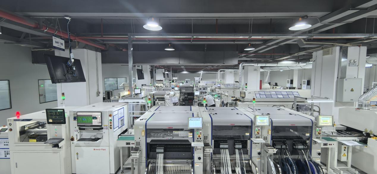
- Production facilities at KING FIELD include 7 SMT lines, 3 DIP lines, 2 assembly lines, and 1 painting line. We have the YSM20R, a machine with placement accuracy ±0.015mm and small-component handling capabilities down to 01005. Our SMT daily capacity is 60 million points, and DIP daily capacity is 1.5 million points.
l A sound quality control system
- Process of quality control
- First, after the engineering documents are processed, as part of a chain of quality control, wax paper is printed and QC checks are done. Following that, production compares the wax paper with the documents, cuts the stencil, and a final inspection is held before shipping. This multi-layer quality control system not only guarantees consistent quality but also reassures customers.
- Concerning quality assurance, KING FIELD has the major six certified systems, IATF 16949, ISO 13485, ISO 9001, ISO 14001, ISO 45001, and QC 080000. By making use of an intelligent MES system that also includes 7 SPI, 7 AOI, and 1 X-Ray types of equipment, we ensure the quality and traceability of every PCBA with shared full traceability.
- We own one of the well-equipped local laser cutting units that are very precise with ±20μm accuracy. Our lasers are IPG from Germany, and we cut at a thickness of 0.03-0.3mm. Besides the fact that this makes us capable of timely delivery, it also allows us to maintain the good overall quality.
- Raw materials and after-sales support
- We exclusively use imported Japanese 304 stainless steel which is distinguished by very high hardness, resistance to heat, and easy cleaning features.
- On top of that, to closely monitor each project and constantly report the progress to the customers, we implemented the system of account managers for each customer.
- In most cases our after-sales team answers within 2 hours and can solve 98% of problems on average.
FAQ
Q1. How do we clean and maintain the steel mesh?
KING FIELD: Ideally, use non-corrosive PCB cleaning liquid. Then, take a soft-bristled brush or a lint-free cloth and gently wipe the stencil to ensure moisture is minimized.
Q2. Are your PCB stencils reused?
KING FIELD: Stencils can be potentially reused depending on the recycling method.
Q3. Does your stencil opening design match my PCB pads?
We use the Gerber files and pad design customer supplied, together with IPC standards, and allow you to approve before proceeding with production.
Q4. Which material is best for stencils?
KING FIELD: Usually, stainless steel foil is chosen for the steel mesh material; however, depending on the process, other materials like nickel could also be used.
Q5. Which of your PCB assembly processes require SMT stencils?
KING FIELD: Surface Mount Technology (SMT) assembly processes require stencil use. To do this, the stencil is laid on the PCB, and paste solder is then printed onto the circuit board's pads.