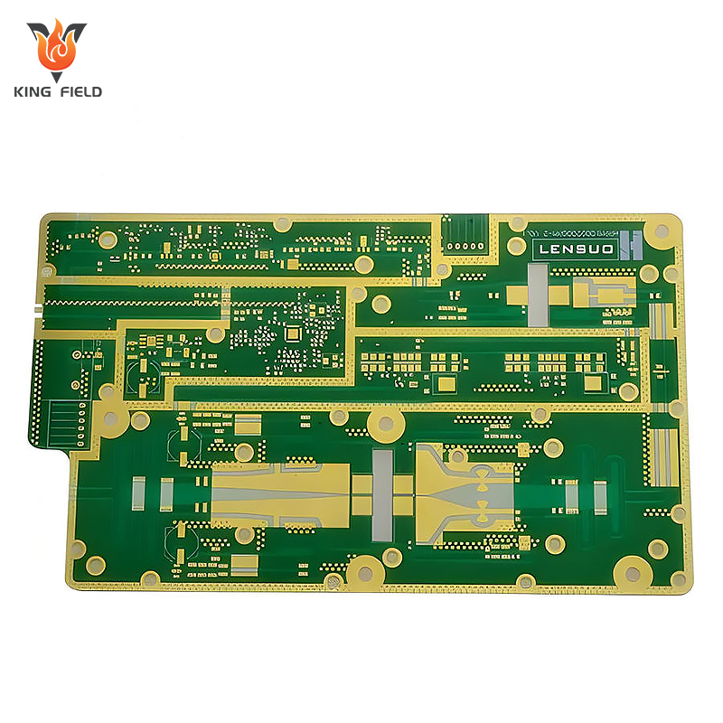
High Frequency PCBs
KING FIELD has twenty years of manufacturing experience in the PCB industry , and we are committed to providing customers with one-stop PCB/PCBA solutions.
☑ Special process: High-density interconnect (HDI, supporting buried vias/blind vias)
☑ Testing methods: Flying probe testing, automated optical inspection
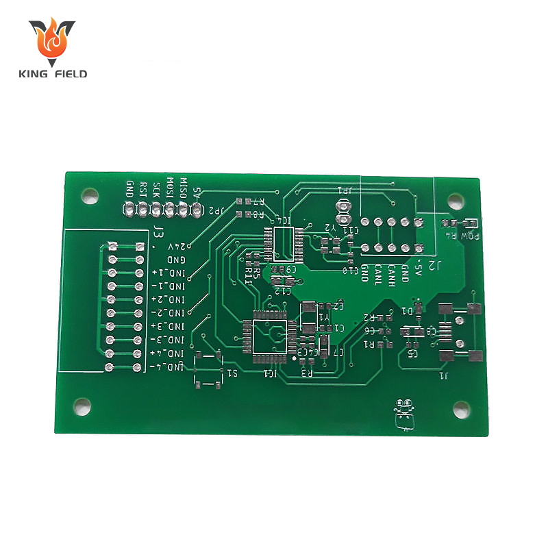
☑ Surface treatment method: Immersion tin , immersion gold, organic solder mask, hard gold, immersion silver, electroless nickel-palladium plating
Description
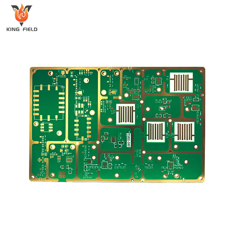
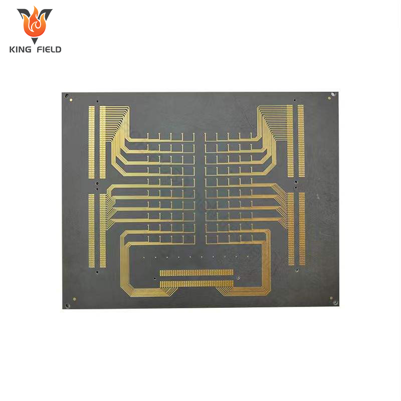
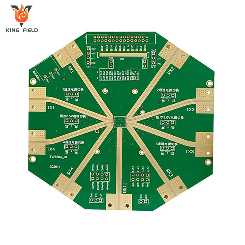
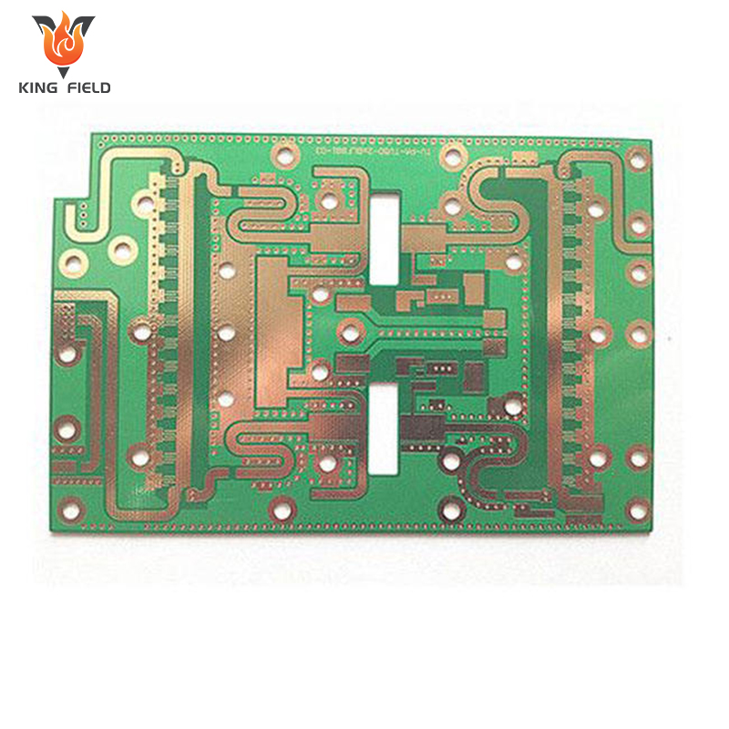
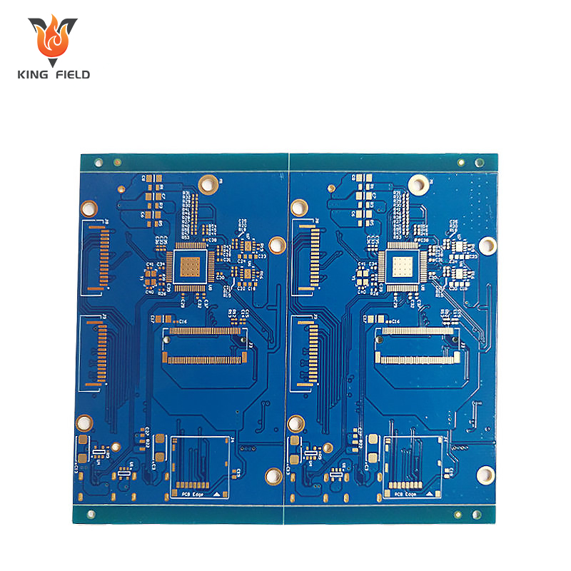
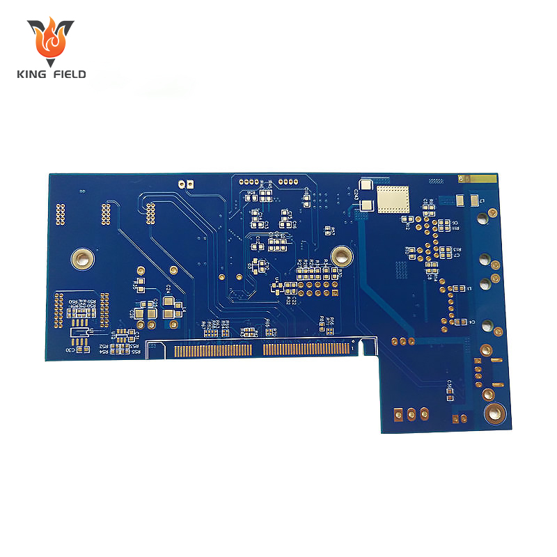
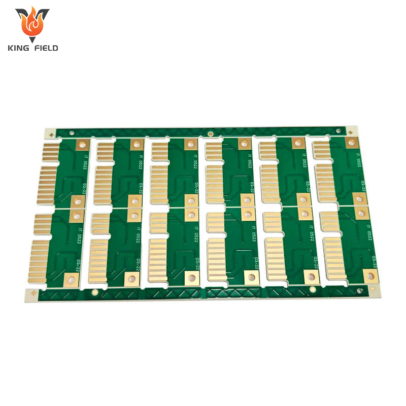
Number of floors: ≥ 4L (4 layers and above can support HDI process)
Substrates: FR-4, aluminum, Rogers, copper-based
Plate thickness: 1.6mm
Copper thickness: 1z
Surface treatments: Immersion gold, immersion tin , gold plating, organic solder mask, hard gold, silver plating, electroless nickel-palladium plating.
thickness: 0.05um
Outer layer line width/spacing: 100/100um
Minimum aperture: 0.2mm
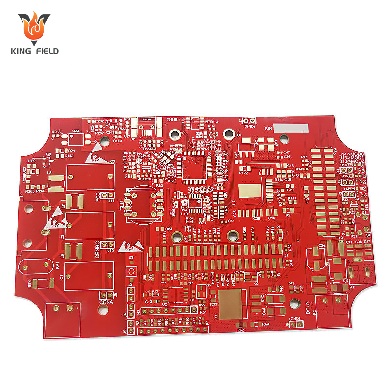
Solder mask character color: Red paint with white lettering
Special process: High-density interconnect (HDI, supporting buried vias/blind vias)
What is a high-frequency PCB?
A PCB with a high-frequency, also termed as the high-frequency PCB board or high-frequency PCB circuit board, is one kind of PCB boards made from a high-frequency PCB material. It has the characteristics of high frequency, high reliability, low latency, big capacity, and high bandwidth.
High-frequency PCBs are widely used in 5G communications, such as 5G base stations and large computer motherboards.
High-frequency PCB circuit boards are also one of KING FIELD 's core products, providing users with design, prototyping, manufacturing, and SMT assembly services for high-frequency PCB circuit boards.
KING FIELD's high-frequency PCB manufacturing capabilities
Characteristic |
Range of capabilities |
Substrate: |
FR-4, aluminum, Rogers, copper-based |
Dielectric constant: |
2.55 |
Outer copper foil thickness: |
1z |
Surface treatment method: |
Immersion tin , immersion gold, organic solder mask, hard gold, immersion silver, electroless nickel-palladium plating |
Minimum line width: |
1.18MM |
Application areas: |
Telecommunications industry |
Shelves: |
2nd floor |
Plate thickness: |
0.2-3.2 MM |
Inner copper foil thickness: |
1z |
Minimum aperture: |
0.15 mm |
Minimum line spacing: |
0.32MM |
Features: |
High-frequency substrate, low dielectric constant |
Solder resist color |
Green, red, yellow, blue, white, black, purple, matte black, matte green |
silkscreen color |
White, Black |
Via process |
Through hole capping, through hole plugging, through hole not capping |
Testing methods |
Flying probe testing, automated optical inspection |
Minimum order quantity |
50 pieces |
Production cycle |
7-10 days |
Expedited delivery cycle |
2-3 days |
KING FIELD 's advantages as a well-known Chinese PCB manufacturer
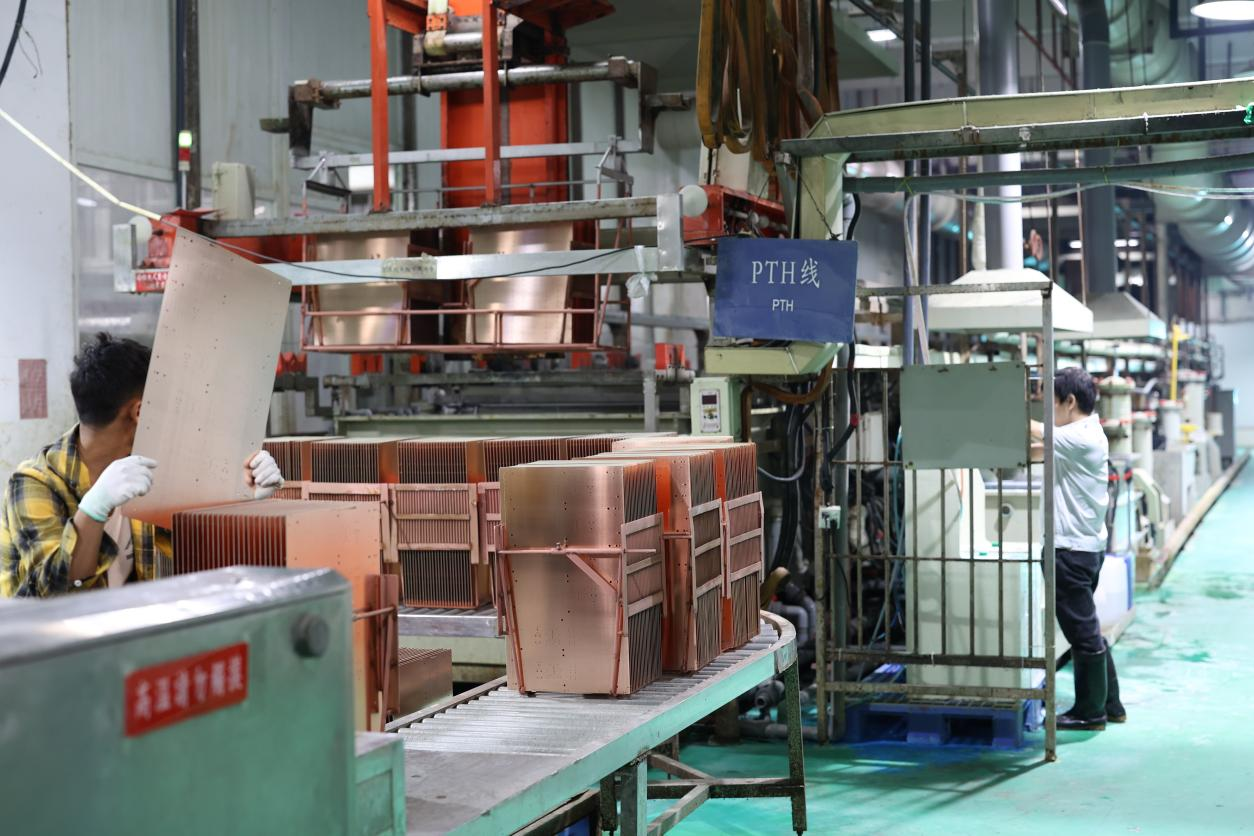
With over 20 years of experience in the PCB/PCBA industry, KING FIELD focuses on the design and production of high-end circuit boards and is committed to providing customers with professional and efficient one-stop PCB/PCBA solutions.
Prototype PCB Assembly
- 100% perfect quality assurance
- Minimum order quantity is flexible
- One stop turnkey manufacturing and assembly service
- Exclusive full service
- Deliver on time
- Rapid mass production capability
- Designing PCB
- Ability to produce
- Parts procurement (only 100% genuine parts)
- Testing and Quality Inspection
- Final assembly
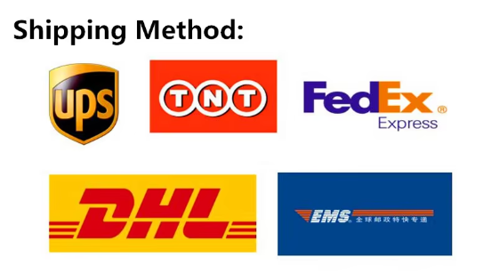
Ways of delivery
Global Delivery: We have established stable and reliable air/sea freight door-to-door services that are perfectly suited for exports to leading markets of Europe, America, and Japan.
KING FIELD After-Sales Service:
Our life long care for your Printed Circuit Board(PCB)
1. Quick response, and great accountability
We guarantee that within 24 hours you will receive our response that is both meaningful and provides a solution in case there is any feedback on process or quality.
2. Locate the source of the problem and take full responsibility
- We have the MES system that supports the comprehensive traceability of the batch manufacturing process for each PCB/PCBA.
- After confirmation of our responsibility, we will cover the entire redoing, repair and round trip logistics costs.
FAQ
Q1: What are the main differences between the high-frequency boards and the ordinary PCBs?
KING FIELD: High-frequency boards are made of very special low-loss materials. For example, an ordinary FR4 material has a signal loss of 0.02dB/cm at 1GHz.
Q2: How do you make a PCB design high-frequency compatible?
KING FIELD: High-frequency characteristics in the PCBs can be obtained through a very careful design of the number of circuit board layers, trace width, stack-up structure as well as the selection of the materials.
Q3 : How do you guarantee the accuracy of your impedance control ?
KING FIELD : We will reserve etching compensation based on a database of 500+ projects . At the same time, we will use LDI+ etching parameter optimization , and then conduct TDR sampling full testing on the first version of each product.
Q4: How long is your high-frequency PCB production cycle?
KING FIELD: Sample : 5-7 days (3 days for rush orders) ; Small batch : 10-15 days ; Large batch : 15-25 days. Note: Special processes (mixed pressing/special surface treatment/full set of S-parameter testing) require an additional 3-10 days.
Q5: How do you handle vias to reduce signal reflection ?
KING FIELD : We shorten the signal return path by using small-diameter vias and then placing vias close to the signal vias, followed by back-drilling to remove excess residue from the vias .