PCB Assembly Process
KING FIELD is a PCBA manufacturer with over 20 years of professional experience. We are committed to providing customers with one-stop PCB/PCBA solutions.
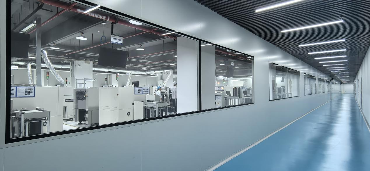
☑ Our SMT production capacity can reach 60,000,000 chips/day.
☑ Mass production can be completed in 10 days to 4 weeks.
☑ 20+ years of industry experience, independently developed MES system
Description
What is the PCB assembly process?
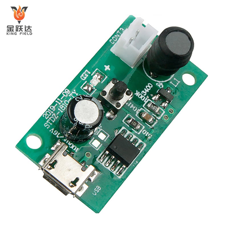
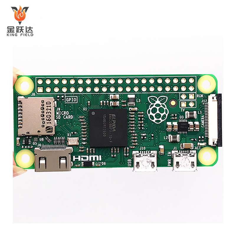
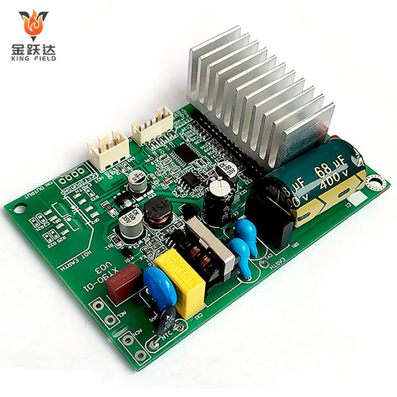
The printed circuit board assembly process basically means soldering or mounting the different kinds of electronic components on a printed circuit board. It is the procedure through which a bare PCB is turned into a fully operational circuit board that can be integrated in electronic devices.
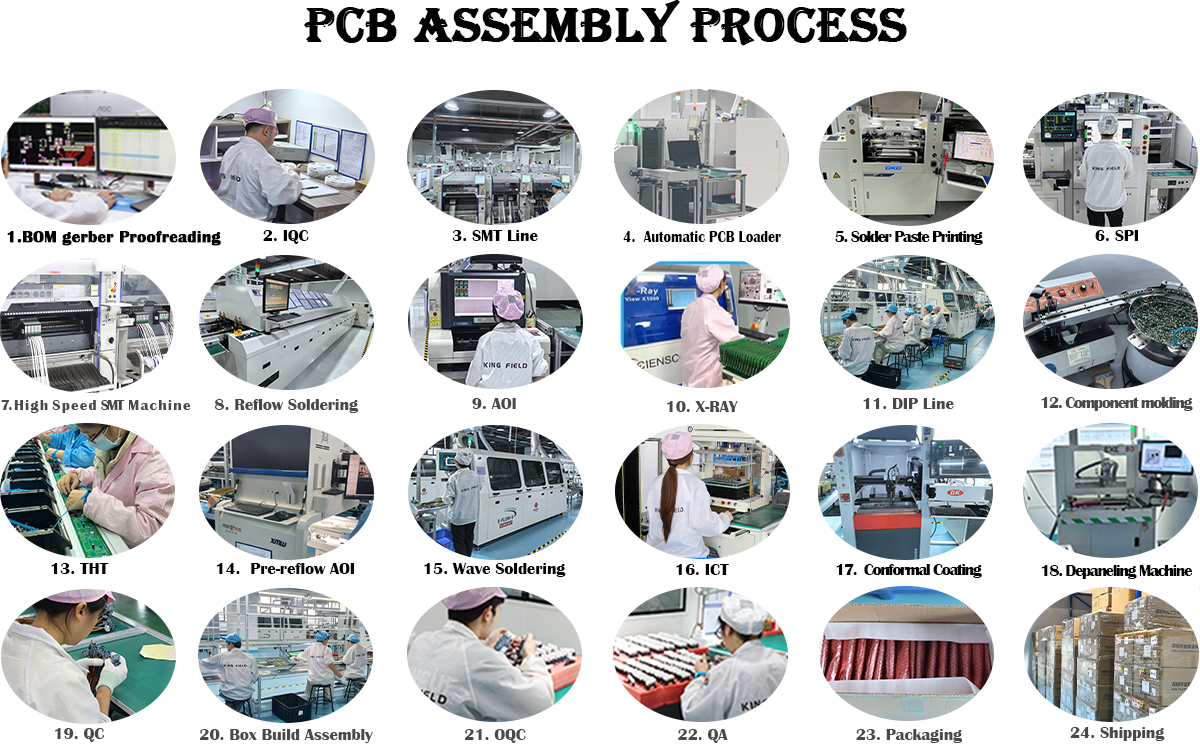
KING FIELD's PCB Assembly Process
Step 1: Incoming Material Inspection
Before we start with PCB assembly, all bare PCB boards, components, solder paste and other materials undergo incoming inspection to make sure they are as per specifications and defective products are prevented from entering production line.
Step 2: Surface Mount Technology (SMT) Assembly
You start with the biggest PCB assembly stage: surface mount technology (SMT) assembly - once everything is ready, such as documents, fixture, or other auxiliary materials.
- Printing solder paste : Using a fully automatic printing machine, solder paste is applied accurately to the PCB pads.
- SPI inspection : 3D solder paste inspection is one of the methods used for checking printing quality.
- Component placement : Our high-speed pick-and-place equipment is used to accurately place the components on their respective positions on the PCB.
- Reflow soldering : The solder paste is melted and the components are firmly soldered onto the PCB.
- AOI : After reflow soldering, inspection is carried out to assess the quality of the soldering and to ensure that the components have not shifted .
- X-ray inspection : The inspection of solder joints that are not visible on the surface is done with this equipment.
- Wave soldering : The PCB may be wave-soldered by coming into contact with molten solder wave; the solder sticks to the exposed metal areas.
- Flying Needle Test (FPT)
Step 3: Through-hole mounting (PTH) assembly
Prepare tooling fixtures → Insert component leads into PCB holes → Wave soldering : After component insertion, the PCB undergoes wave soldering, where molten solder forms waves that contact the component leads to complete the soldering; high-density boards use selective wave soldering. → Trim excess leads.
Step 4: Panel cleaning
Step 5: Functional Testing (FCT)
Step 6: Apply conformal coating
Step 7: Packaging and Shipping
FAQ
Q1. How do you avoid cold solder joints, bridging, and missing solder joints?
KING FIELD: We adopt the standard SMT process flow, and then use AOI optical inspection and X-Ray inspection. The first piece full inspection + process inspection + final inspection of finished products are triple-checked to prevent defects such as cold solder joints, bridging, and missing solder from the source.
Q2. How do you guarantee stable delivery times and avoid delaying our project's mass production?
KING FIELD: Production will be started once the order is confirmed and we will produce your order simultaneously with your schedule in time. Expedited orders will be prioritized and we will strictly deliver the goods according to the agreed delivery date.
Q3. How do you manage and prevent incorrect materials, loss, and excessive waste?
KING FIELD: Our MES system enables full traceability of the manufacturing process for each PCB/PCBA. In addition, any leftover materials from our production will be collected and returned unopened.
Q4. How do you ensure the soldering reliability of precision components such as BGA and QFN?
KING FIELD: High-precision reflow soldering is our means to strictly control the temperature profile to ensure the soldering reliability of precision components.
Q5. How do you handle quality issues that arise after shipment?
we will respond within 24 hours and provide corresponding analysis reports and repair services.