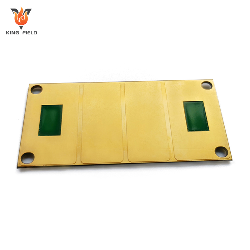
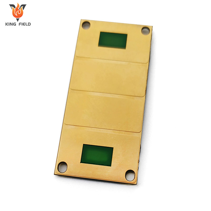

Ceramic PCB
With over 20 years of experience in PCB prototyping and manufacturing , KING FIELD prides itself on being your best business partner and close friend, meeting all your PCB needs.
☑ Supports advanced processes such as laser drilling, metallization, and immersion gold plating.
☑ A variety of ceramic substrates are available, including alumina, aluminum nitride, and Si₃N₄.
☑ With a thermal conductivity as high as 170 W/m·K, it effectively reduces the chip's operating temperature.
Description
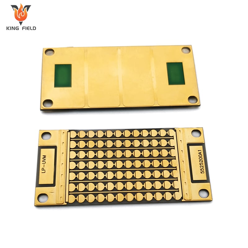
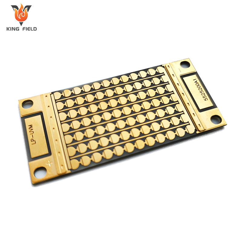
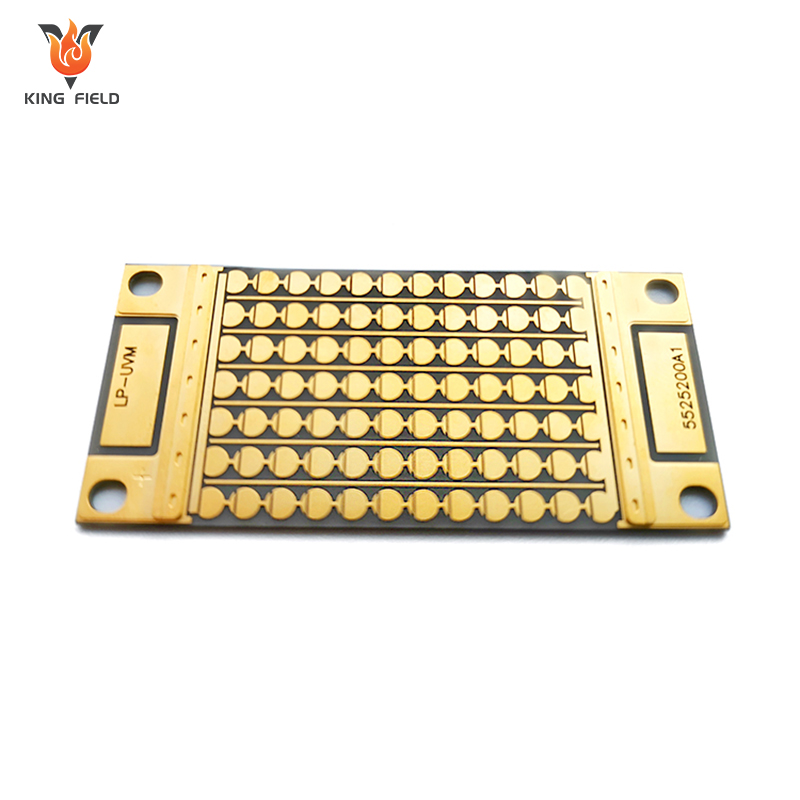
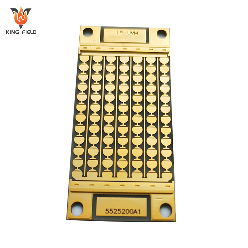
What is a ceramic PCB?
Ceramic printed circuit board are electronic packaging substrates with ceramic materials as the base, primarily using ceramic materials (usually aluminum-based materials). These circuit boards have excellent thermal conductivity, electrical insulation, and mechanical strength, so they can be widely used in high-reliability scenarios such as new energy vehicles, optoelectronics, 5G communications, and industrial control.
Material: Ceramic
Number of floors: 2
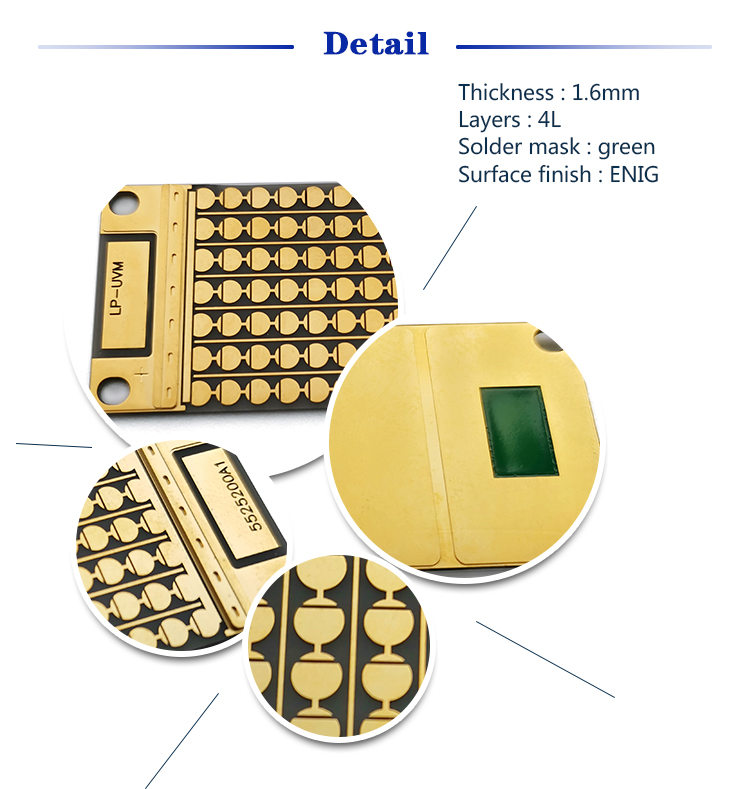
Craftsmanship: Immersion gold
Minimum drill hole: 0.3mm
Minimum line width: 5mil
Minimum line spacing: 5mil
Features: High thermal conductivity, rapid heat dissipation
KING FIELD's ceramic pcb board manufacturing capabilities
Technical dimension |
KING FIELD's capabilities |
substrate |
ceramics |
Outer copper foil thickness |
1z |
Surface treatment methods |
Immersion gold , immersion silver, electroless nickel-gold plating (ENIG), electroless nickel-palladium-gold plating (ENEPIG), or organic solder mask (OSP) |
Minimum line width |
5mil |
Shelves |
2nd floor |
Plate thickness |
2.6mm |
Inner copper foil thickness |
1-1000 micrometers (approximately 30 ounces) |
Minimum aperture |
0.05±0.025 mm |
Minimum line spacing |
2/2 mil |
Maximum size |
120×120 mm |
Drilling and through-hole capabilities |
Round and square plated holes and slots; electroplating and filling; half-hole and side plating. |
Solder resist color |
Green, blue, white, black |
Features |
Ceramic plate, high thermal conductivity, rapid heat dissipation |
Precision circuits |
4/4mil ultimate accuracy |
Plate thickness coverage |
All models from 0.38-2.0mm |
Copper Thickness Customization |
Flexible configuration from 0.5 to 3.0 oz |
Industry and Application |
Smart lighting, biomedicine, renewable energy, telecommunications & 5G, power electronics, automotive electronics |
Choose KING FIELD: the most reliable ceramic PCB supplier!
Although KING FIELD was founded in 2017, our core technology team has more than 20 years of experience in the PCB manufacturing field .
20 years of mature experience in ceramic PCB manufacturing
Our core team has 20 years of mature experience in ceramic PCB manufacturing and has provided high-quality services to many customers with ceramic PCB manufacturing needs.
We have built a small-to-medium batch production line and a complete process control system , which ensures process precision while enabling rapid response to customers' mass production needs . Our core advantages include:
Process capabilities
Precision laser processing : Laser drilling diameter accuracy ±15μm, cutting accuracy ±25μm , supporting high-end processes such as laser drilling, metallization, and immersion gold.
High thermal conductivity : Our ceramic PCB has a thermal conductivity of up to 170W/m·K, which effectively reduces the chip's operating temperature.
Excellent high temperature resistance : Suitable for extreme environments up to 800°C, with stable performance.
Preferred material systems : A variety of ceramic substrates can be selected, such as alumina, aluminum nitride, and Si₃N₄.
Export performance
Our production system has passed ISO 9001:2015 and IATF 16949 certifications. Our products have long been exported to high-end manufacturing regions such as Germany, the United States, Switzerland, and Japan , and are mainly used in:
High-power laser/LED heat dissipation substrate
Aerospace sensor modules
Core circuit of medical imaging equipment
New energy vehicle power module
FAQ
Q1 . Is it possible to manufacture ceramic PCBs with plated through-holes?
KING FIELD: Yes. DPC technology is ideal for creating ceramic PCBs with plated vias and interconnect structures for a variety of ceramic materials.
Q2. How do you achieve high-precision metallization on ceramic surfaces?
KING FIELD: We use laser texturing and plasma activation , and then optimize the process parameters for thick/thin films to ensure peel strength and thus achieve high-precision metallization.
Q3.How to achieve reliable interlayer interconnection in ceramic multilayer substrates?
KING FIELD: We use laser precision drilling and vacuum filling to ensure a fill rate of ≥98% . Then, we combine optical stacking alignment with isostatic pressing and controlled co-firing processes to ensure the alignment accuracy between layers .
Q4 . How do you control the thermal conductivity and coefficient of thermal expansion of ceramic substrates?
KING FIELD: We use high-purity materials and precise formulations, and optimize the sintering curve and atmosphere to achieve stable output of thermal conductivity.
Q5 . How are ceramic PCBs cut and shaped?
KING FIELD: The shape of the ceramic PCB (including drilling) is cut using high-power precision lasers such as fiber lasers. Although ceramics have high mechanical strength, they are inherently brittle, and drilling and milling can easily lead to ceramic chipping, cracking, or excessive tool wear.