
 EN
EN
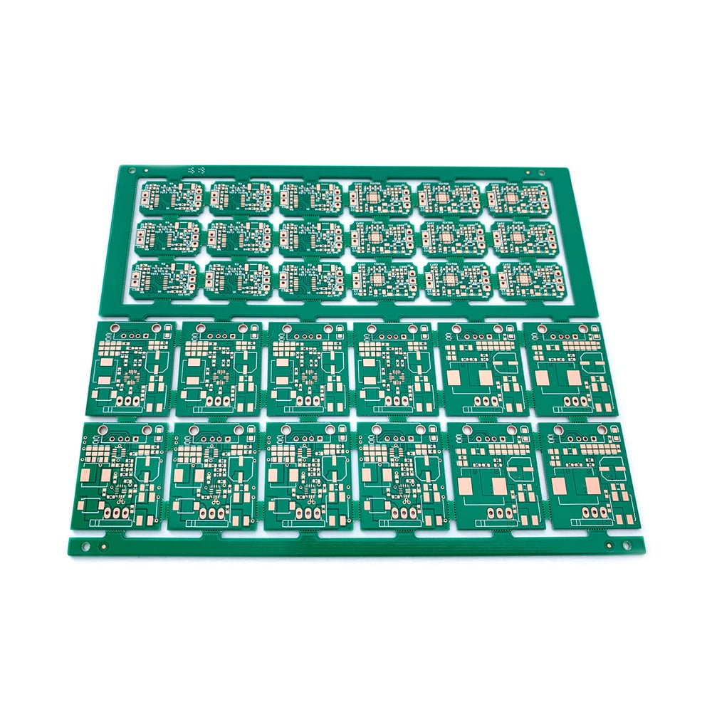
Thermal Management for Stable Double Sided PCB Soldering
Balancing Heat Distribution Across Both Layers
Effective thermal management starts with even heat distribution across both sides of the assembly. During reflow, temperature imbalances can cause one layer to reach liquidus while the other remains below reflow temperature—leading to cold joints or tombstoning. Designers use several proven techniques to equalize the thermal profile. High-mass components—such as large BGAs or power inductors—are offset from each other on opposite layers to prevent localized heat sinking. Thermal vias—plated through-holes filled with conductive material—actively transfer heat from top to bottom, promoting uniform heating. Strategic copper pours and ground planes further spread heat, minimizing surface gradients. A symmetric PCB stack-up also ensures both sides receive equivalent thermal mass during dual-reflow processing. These practices ensure solder paste on both sides reaches proper reflow temperature simultaneously, enabling reliable wetting and strong intermetallic bond formation—critical for high-yield double sided PCB soldering in dense, mixed-technology designs.
Mitigating Warpage and Thermal Stress During Dual Reflow
Exposing a PCB to two reflow cycles intensifies warpage and residual thermal stress risks. Gradual heating and cooling help control board movement, preventing delamination, lifted pads, or cracked vias. Laminates with a glass transition temperature (Tg) above 170 °C maintain dimensional stability through peak reflow temperatures. Pre-heat ramp rates of 1–3 °C/s minimize thermal shock and allow uniform board equilibration before entering the reflow zone. Many manufacturers use reflow carriers to physically restrain panels, holding warp within the 0.75% limit defined byfor rigid boards. Controlled cooling—typically 2–4 °C/s—avoids quenching that could lock in internal stress, especially in large BGA components. Early use of thermal simulation tools identifies high-stress zones and informs fixture or profile adjustments. Together, these steps preserve joint integrity and are indispensable for maintaining reliability across repeated thermal cycles.
Precision Stencil Design and Solder Paste Control for Double Sided PCB Soldering
Achieving Consistent Paste Volume on Top and Bottom Layers
Ensuring uniform solder paste deposit on both layers is critical for reliable double sided PCB soldering. Precision stencil design dictates deposition accuracy. The aperture area ratio—the ratio of aperture opening area to its wall area—must exceed 0.66 for clean paste release, especially for fine-pitch components common in dense double-sided assemblies. Aspect ratio (width-to-thickness) should be ≥1.5 to prevent clogging. A stencil thickness of 0.1–0.15 mm is typical, though dual-layer designs may benefit from step stencils to deliver more paste to larger thermal pads on one side without over-pasting fine-pitch areas on the other. Automated Solder Paste Inspection (SPI) after each side’s printing quantifies volume, height, and alignment; integration of SPI has been shown to reduce bridging defects by up to 80% [SMTA Benchmark Report, 2023]. Inconsistent paste on the bottom layer increases risks of tombstoning and open joints after secondary reflow. Squeegee parameters—speed 20–30 mm/s, pressure 10–15 N, and separation speed 1–3 mm/s—stabilize paste release across varied pad geometries. These controls ensure first-side paste integrity during the second print cycle, directly supporting double sided PCB soldering yield.
Sequential Reflow Strategies to Maximize Double Sided PCB Soldering Reliability
Optimizing First-Pass and Second-Pass Reflow Profiles
Reliable double sided PCB soldering demands a deliberate split in how the A-side and B-side reflow profiles are engineered. On the first pass, the oven must bring the entire assembly—bare board and all components—to full liquidus for robust initial joint formation. Industry-accepted profiles for SAC305 solder target a peak temperature of 240–250 °C, with time-above-liquidus (TAL) of 60–90 seconds. For the second pass, the goal shifts: achieve solid B-side joints while avoiding re-melting of A-side joints to the point of collapse or thermal damage. This requires a slightly lower peak temperature (235–245 °C), faster ramp-to-peak, and reduced TAL—lowering total heat load on the bottom layer. A 2023 process study found that reducing second-side TAL by just 15% cut board warpage incidence nearly in half. Controlled cooling at 2–4 °C/s prevents thermal shock and grain coarsening, preserving joint integrity. The table below illustrates typical parameter shifts between passes.
| Reflow Parameter | First‑Pass (A‑Side) | Second‑Pass (B‑Side) |
|---|---|---|
| Preheat ramp rate | 1.5–2.5 °C/s | 2.0–3.0 °C/s (quicker soak) |
| Soak zone (150–160 °C) | 90 s | 60–80 s |
| Peak temperature | 240–250 °C | 235–245 °C (lower risk of A‑side reflow) |
| Time above liquidus (TAL) | 70–90 s | 55–75 s |
| Cooling rate | 2–3 °C/s | 2–4 °C/s (faster, controlled cool-down) |
Maintaining such precisely tapered profiles across both cycles guards against latent defects—including cracked BGA spheres, brittle intermetallics, and delamination—that compromise long-term reliability.
Why ‘Flip‑and‑Reflow’ Fails Without Fixturing: Solving the Component Retention Paradox
Flipping a board for second-pass reflow places heavy components on the bottom side, held in place only by the tackiness of uncured solder paste. Gravity, conveyor vibration, and rapid thermal expansion inside the oven can dislodge parts as large as QFP-208s or BGA-484s—a phenomenon production engineers call the component retention paradox. A leading EMS provider documented a 0.8% per-assembly fall-off rate for bottom-side BGAs without mechanical support (2022), rendering unassisted flip-and-reflow unsuitable for high-yield manufacturing. The physics is clear: paste tack forces (often <2 N for a 1 mm² pad) compete with component weight that can exceed 20 g under elevated temperatures. The solution is dual-pronged. First, light-cure or heat-cure adhesives are dispensed between component bodies and the PCB surface to lock large packages in place. Second, custom high-temperature fixtures—built from low-thermal-mass alloys or ceramics—support the board from below, neutralizing droop and vibration. When optimized fixturing is deployed alongside a de-tuned second-pass profile, drop rates fall to zero and first-pass yields exceed 99.5%. For double sided PCB soldering relying on simple flip-and-reflow, this paradox remains the most direct threat to repeatable reliability.
Fixture-Assisted Double Sided PCB Soldering: Enabling Repeatable, High-Yield Production
Designing and Selecting High-Temperature Fixtures for Dual Reflow Cycles
In double sided PCB soldering, the second reflow cycle places first-pass components in an inverted, gravity-dependent state. A well-engineered fixture prevents displacement and tombstoning by delivering rigid, low-thermal-mass support. Material choice is critical: titanium alloys and high-performance composites maintain dimensional stability up to 260 °C while resisting oxidation and flux attack. Fixture design must incorporate milled pockets that cradle bottom-side components without obstructing thermal airflow—and precise registration pins to guarantee repeatable board alignment across hundreds of cycles. Insufficient clearance or excessive fixturing mass can trap heat, distort the reflow profile, and increase defect rates. By balancing mechanical retention with thermal uniformity, high-temperature fixtures transform flip-and-reflow from a high-risk manual step into a controlled, high-yield process.
FAQs: Answering Common Questions About Double Sided PCB Soldering
What is the advantage of using thermal vias in double sided PCB soldering?
Thermal vias help transfer heat effectively between the top and bottom layer of a PCB, ensuring uniform temperature distribution during reflow cycles. This prevents cold joints and promotes reliable soldering.
Why are asymmetric reflow profiles critical in double sided PCB soldering?
Asymmetric reflow profiles help protect previously soldered components during the second reflow by utilizing slightly lower peak temperatures and optimized parameters for reduced stress and defect prevention.
How do fixtures assist in double sided PCB soldering?
Fixtures provide mechanical stability and support during second-pass reflow, preventing component displacement due to gravity, vibration, or thermal expansion while ensuring uniform thermal distribution.
What role does solder paste inspection (SPI) play in double sided PCB soldering?
SPI ensures consistent solder paste volume, alignment, and height, reducing bridging defects and improving the reliability of double sided soldering processes.
Can adhesives alone solve component retention during flip-and-reflow?
While adhesives help secure components, they are more effective when combined with high-temperature fixtures that provide physical support and minimize environmental vibrations during the reflow process.
Table of Contents
- Thermal Management for Stable Double Sided PCB Soldering
- Precision Stencil Design and Solder Paste Control for Double Sided PCB Soldering
- Sequential Reflow Strategies to Maximize Double Sided PCB Soldering Reliability
- Fixture-Assisted Double Sided PCB Soldering: Enabling Repeatable, High-Yield Production
-
FAQs: Answering Common Questions About Double Sided PCB Soldering
- What is the advantage of using thermal vias in double sided PCB soldering?
- Why are asymmetric reflow profiles critical in double sided PCB soldering?
- How do fixtures assist in double sided PCB soldering?
- What role does solder paste inspection (SPI) play in double sided PCB soldering?
- Can adhesives alone solve component retention during flip-and-reflow?

