
 EN
EN
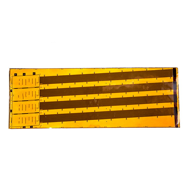
Superior Space Efficiency and 3D Design Integration
Maximizing Packaging Density with Dynamic 3D Layout Optimization
Flexible rigid PCBs unlock unprecedented space efficiency by enabling electronics to occupy three-dimensional volumes—something planar rigid boards cannot achieve. Rather than spreading circuits across a flat surface, designers fold and bend flexible sections to conform precisely to the product’s enclosure geometry. This dynamic 3D layout allows stacking and nesting of functional layers in air space previously left unused, often reducing total packaging volume by up to 60% compared to rigid-board-plus-cable assemblies (2023 industry benchmark). In wearables, this means curving seamlessly around the wrist; in compact medical devices, it enables folding complex circuitry into capsule-like enclosures. The result is a single, integrated 3D circuit assembly that maximizes functional density without increasing external footprint.
Eliminating Connectors and Cables Through Monolithic Interconnect Integration
Flexible rigid PCBs eliminate bulky wiring harnesses and mating connectors—the primary sources of wasted internal volume and weight in multi-board systems. Every solder joint, crimped pin, and connector housing consumes space and introduces mechanical clearance constraints. Replacing these discrete interconnects with a continuous, monolithic flex circuit transforms the design from a collection of wired boards into one unified structure. A thin polyimide flex layer—often thinner than a sheet of paper—bridges rigid sections with high-density, low-profile routing. This integration frees up cavities and contours previously reserved for cable bend radii or connector clearance, enabling sleeker industrial designs and creating room for larger batteries or additional feature-dense modules within the same envelope.
Enhanced Reliability and Mechanical Durability
Dynamic Bend Reliability in Flexible Rigid PCBs: Air-Gap Designs and Strain-Relieved Flex Zones
Dynamic flexing rapidly degrades conventional interconnects—but flexible rigid PCBs are engineered for motion. Two key structural strategies ensure long-term reliability: air-gap construction, which removes rigid material from bending regions to allow unrestrained flex-layer movement, and strain-relieved flex zones, where trace widths taper, corners round, and copper is aligned to the neutral axis to minimize stress concentration. When combined, these features enable over 100,000 bending cycles without trace cracking or delamination, as validated in a 2023 avionics-grade reliability study. This performance is essential in applications like folding surgical instruments, drone gimbals, and automotive radar hinges—environments where ribbon cables would fail quickly under repeated motion. By embedding mechanical resilience directly into the stack-up, rigid-flex assemblies deliver predictable, field-proven durability.
Fewer Failure Points: ZIF Tails and Seamless Rigid-to-Flex Transitions vs. Soldered Cables
Discrete connectors and solder joints remain the most frequent failure points in bend-prone electronics. While Zero Insertion Force (ZIF) tails reduce mechanical stress at interfaces, contact fretting and latch wear still limit lifecycle reliability. The greatest reliability leap occurs when rigid-flex design eliminates all interconnections along the flex path.
| Connection Method | Typical Failure Modes | Dynamic Reliability |
|---|---|---|
| Soldered cables | Solder joint cracking, wire fatigue | 5% failure rate after 1,000 cycles |
| ZIF connectors | Contact fretting, latch wear | 1% failure after 10,000 cycles |
| Monolithic rigid-to-flex transition | None – continuous copper | Zero discrete failure points |
A seamless rigid-to-flex transition creates a single, uninterrupted copper path—no solder joints, no separable contacts, no stress risers. In vibration and thermal cycling tests simulating automotive under-hood conditions, monolithic transitions showed zero interconnect-related failures after 20,000 cycles, while soldered cable assemblies exhibited a 7% failure rate (Reliability Engineering Review, 2022). This inherent robustness slashes field returns, simplifies root-cause analysis, and makes rigid-flex the preferred architecture for mission-critical systems.
Long-Term Cost and Assembly Efficiency Gains
Flexible rigid PCBs consolidate multiple rigid boards and flex layers into a single, unified assembly—reducing component count, eliminating manual wiring steps, and cutting assembly time by up to 50% in high-mix production. With interconnects etched directly into the flex layers, there’s no risk of miswired connectors or loose cables, reducing test time and rework. A leading automotive electronics supplier reported a 20% reduction in total installed cost after transitioning to rigid-flex, citing fewer hand-soldering operations and a 30% drop in field returns tied to interconnection failures. Over the product lifecycle, the absence of solder joints and crimp pins extends mean time between failures (MTBF), lowering warranty costs and unplanned downtime. Accelerated validation via 3D virtual prototyping—and substrate reuse across product families—further amplifies economic value, more than offsetting the modest upfront fabrication premium.
Optimized Electrical Performance and EMI Mitigation
Maintaining Controlled Impedance Across Rigid‑Flex Boundaries
Signal integrity in flexible rigid PCBs relies on consistent impedance control at the rigid-to-flex transition. Unlike board-to-board connectors—which introduce abrupt dielectric changes and discontinuities—a monolithic construction maintains a continuous reference plane across the bend. Trace width adjustments tailored to the flex-region stackup preserve target impedance (e.g., 50 Ω single-ended or 100 Ω differential), keeping return paths intact. This approach limits signal reflections to below −25 dB and sustains clean eye diagrams even at multi-gigabit data rates—critical for high-speed digital and RF applications.
Integrated EMI/RF Shielding Using Ground Planes and Conductive Coverlays in Flexible Rigid PCBs
Flexible rigid PCBs integrate EMI mitigation directly into the build. Solid copper ground planes on outer flex layers serve as low-impedance return paths that confine electric fields close to signal traces. Conductive coverlays—such as silver-ink films or copper-clad polyimide—form a continuous, laminated barrier against radiated emissions. Because shielding is embedded—not added as a separate metal can or gasket—it avoids mass penalties and eliminates failure-prone mechanical contacts. This architecture meets stringent EMC standards like CISPR 32 without extra assembly steps or trade-offs in dynamic bend performance.
FAQ Section
What are flexible rigid PCBs?
Flexible rigid PCBs are circuit boards that combine both flexible and rigid sections into a single assembly, allowing for 3D layouts and integration.
How do flexible rigid PCBs maximize space efficiency?
They enable the folding and bending of flexible layers, allowing functional stacking within the enclosure geometry and reducing unused air space.
What reliability benefits do flexible rigid PCBs offer over soldered cables?
They eliminate failure points such as solder joints or separable contacts, offering over 100,000 bending cycles with reduced failure rates.
How do flexible rigid PCBs reduce costs in production?
By consolidating components and eliminating manual wiring, they improve assembly time and reduce field returns and warranty costs.
What advantages do they offer for EMI mitigation?
Embedded ground planes and conductive coverlays ensure compliance with EMC standards while maintaining lightweight, compact designs.

