
 EN
EN
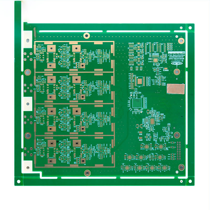
HDI Flex PCB Enables Extreme Miniaturization in Space-Constrained Designs
As electronics shrink, designers face the challenge of packing more functionality into ever-smaller volumes. HDI flex PCB technology directly addresses this by combining microvias, fine traces, and flexible substrates to achieve industry-leading component density while maintaining reliability in the most restricted spaces.
Microvias and Coreless Construction for Ultra-Compact Layouts
Microvias—laser-drilled holes under 0.15 mm in diameter—are the foundation of HDI flex miniaturization. They replace traditional through-holes, enabling layer-to-layer signal transitions without consuming surface area. Paired with trace widths as narrow as 0.075 mm, they support routing densities that reduce board area by up to 30% versus conventional rigid PCBs. Coreless construction amplifies this advantage: instead of stacking on a thick FR4 core, dielectric layers are built sequentially on a temporary carrier. The result is an ultra-thin, multi-layer (10+ layer) flex circuit with exceptional mechanical integrity—ideal for wearables and implantable medical devices where thickness and volume are non-negotiable. Eliminating the rigid core also improves impedance consistency and shrinks signal loop areas, enhancing high-frequency performance. These features allow circuits to bend and fold into 3D assemblies—transforming unused space into functional routing real estate.
BGA Fanout and High-Pin-Count Device Support in Tight Footprints
High-pin-count BGAs with pitches down to 0.4 mm demand precision routing in minimal footprints. HDI flex meets this need with microvia-in-pad technology, placing blind vias directly beneath BGA pads to enable inner-layer escape routing—eliminating large via keep-out zones. This allows over 1,000 pins to be fanned out within a 50 mm × 50 mm footprint. For example, automotive battery management ECUs consolidate processing, power delivery, and CAN/FlexRay interfaces into that same area while preserving signal integrity up to 1 GHz. Stacked and staggered microvias provide robust interlayer connectivity for dense DRAM or FPGA interfaces—often reducing required layers by 2–4 versus rigid alternatives. Crucially, the polyimide substrate absorbs thermal expansion mismatch between silicon and board, a key reliability factor when mounting high-density BGAs on dynamic or thermally cycled surfaces. This capability makes HDI flex the architecture of choice for smartphones, compact IoT gateways, and handheld medical analyzers—where every square millimeter must deliver maximum functional value.
Superior Electrical Performance of HDI Flex PCB in High-Speed Applications
Shorter Signal Paths and Reduced Loss for 5G, Aerospace & Medical Systems
HDI flex eliminates long plated-through holes in favor of laser-drilled microvias—shortening signal paths and slashing parasitic stub length. A 2023 signal integrity study found a typical 12-layer HDI flex design exhibited 40% less insertion loss at 28 GHz than its rigid counterpart, directly improving waveform fidelity. In 5G mmWave antenna arrays, this translates to measurable gains in radiated efficiency; in aerospace telemetry links operating above 10 Gbps, reduced skew across differential pairs prevents bit-error accumulation during vibration. Handheld ultrasound probes benefit too: shorter paths lower EMI susceptibility in sensitive front-end analog chains. Coreless construction supports these advantages by enabling seamless layer transitions within the flex stack—removing bulky rigid-to-flex transition zones that degrade high-frequency behavior. Independent testing (2024) confirmed HDI flex maintains insertion loss below 0.5 dB per inch at 40 GHz, validating its readiness for next-generation high-speed platforms.
Impedance Control and Signal Integrity in Dynamic Routing Environments
Maintaining consistent characteristic impedance during repeated flexing is essential—and achievable with HDI flex. Advanced polyimide dielectrics with ±5 µm thickness tolerance, combined with laser-defined trace geometry, enable stable 50 Ω single-ended and 100 Ω differential routing—even across tight bends. An independent 2022 test lab analysis showed HDI flex boards held impedance deviation under 3% after 100,000 dynamic flex cycles, compared to up to 12% drift in standard flex circuits. This stability is critical for PCIe Gen 4 in industrial cameras and JESD204B in phased-array radars. Coplanar waveguide structures with buried reference planes further suppress crosstalk, measuring below −35 dB at 16 GHz. Where rigid-flex transitions are unavoidable, HDI enables the reference plane to extend continuously through the bend zone—eliminating impedance discontinuities that cause reflection-induced jitter. The outcome is sustained bit-error rates below 10⁻¹², meeting the stringent reliability requirements of aerospace and medical systems—even under continuous mechanical stress.
Enhanced Reliability of HDI Flex PCB Under Mechanical Stress and Harsh Conditions
Vibration Resistance and Bend-Fatigue Performance in Automotive & Wearables
HDI flex excels in dynamic environments—serving as the structural and electrical backbone of modern automotive ADAS modules and wearable health monitors. Its reliability stems from adhesiveless polyimide constructions that eliminate delamination risk and withstand repeated bending far beyond conventional rigid or adhesive-based flex circuits. Critical design practices include avoiding microvia fields in active flex zones to prevent copper cracking, and specifying bend radii aligned with IPC-6013 Class 3 guidelines for dynamic applications. In wearables, a single HDI flex circuit replaces multiple rigid boards and connectors—reducing failure points and achieving a lightweight 0.2 g/cm² form factor. Automotive-grade HDI flex undergoes rigorous qualification—including thermal cycling, mechanical shock, and microsection analysis—to ensure zero-failure operation across temperature extremes and high-vibration conditions. This proven resilience ensures uninterrupted signal integrity for mission-critical functions, from continuous ECG monitoring in smartwatches to real-time image processing in surround-view camera systems.
Advanced HDI Stack-Up Innovations: Microvias, Sequential Lamination, and Rigid-Flex Integration
Blind/Buried Vias vs. Stacked Microvias for Scalable High-Density IoT Devices
Blind and buried vias serve limited Z-axis routing needs in simpler HDI flex designs—but fall short for scalable, ultra-dense IoT edge devices. Stacked microvias—formed via sequential lamination—enable vertical interconnections across multiple build-up layers, dramatically increasing routable density and freeing surface area for fine-pitch BGAs. This enables advanced stack-ups like 2+N+2 and 3+N+3, where staggered microvia patterns mitigate crack propagation under dynamic flexing—especially vital in rigid-flex HDI assemblies using polyimide cores. When paired with microvia-in-pad layouts, stacked microvias support BGAs down to 0.4 mm pitch, a common requirement in sensor fusion hubs and compact wearables. While blind/buried vias remain viable for cost-sensitive, low-complexity applications, stacked microvias have become the de facto standard for next-generation HDI flex—enabling precise dielectric thickness control for impedance tuning and supporting low-loss laminates for GHz-range signal integrity. Ultimately, the choice hinges on balancing density, mechanical reliability, and manufacturability—with stacked microvias delivering the scalability today’s miniaturized IoT demands.
FAQ
What is HDI flex PCB and why is it used?
HDI flex PCB stands for High-Density Interconnect flexible printed circuit board. It is used in miniaturized electronics to achieve high component density and reliable performance in space-constrained designs, thanks to its use of microvias, fine traces, and flexible substrates.
How do microvias enhance the performance of HDI flex PCBs?
Microvias replace traditional through-holes, allowing layer-to-layer signal transitions without taking up surface area. They also enable higher routing densities and contribute to compact layouts critical for miniaturized devices.
What applications benefit most from HDI flex PCB technology?
Applications such as wearable devices, smartphones, automotive systems, medical analyzers, and aerospace telemetry benefit from HDI flex PCB technology due to its space-saving, high reliability, and superior electrical performance.
How does HDI flex PCB handle high-speed signal applications?
HDI flex PCB excels in high-speed applications by shortening signal paths using microvias and coreless construction, reducing insertion loss and ensuring stable impedance, even under repeated mechanical stress or high-frequency operation.
Table of Contents
- HDI Flex PCB Enables Extreme Miniaturization in Space-Constrained Designs
- Superior Electrical Performance of HDI Flex PCB in High-Speed Applications
- Enhanced Reliability of HDI Flex PCB Under Mechanical Stress and Harsh Conditions
- Advanced HDI Stack-Up Innovations: Microvias, Sequential Lamination, and Rigid-Flex Integration
- FAQ

