
 EN
EN
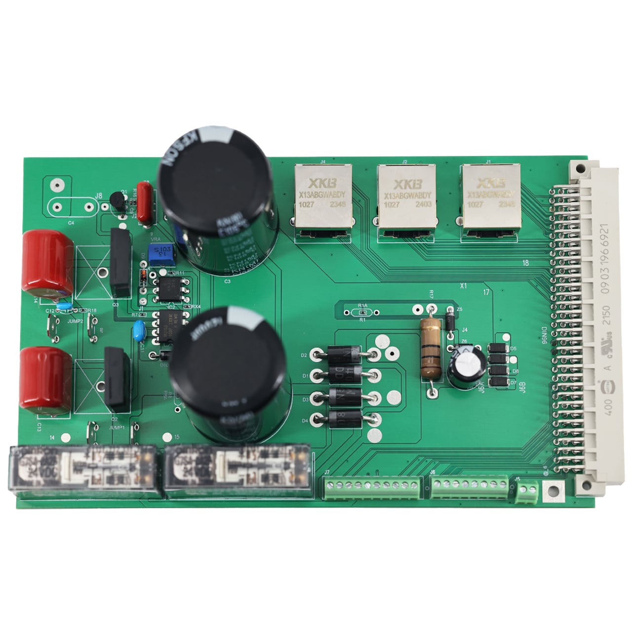
Space Optimization Through 3D Dynamic Routing and Footprint Reduction
Breaking Planar Limits: How Flex PCB Assembly Enables True 3D Packaging
Traditional rigid boards confine design to flat, two-dimensional layouts—wasting valuable enclosure volume. Flex PCB assembly breaks that constraint: thin, bendable polyimide substrates allow circuits to fold, twist, and conform tightly around mechanical structures, turning unused corners into functional zones. Instead of stacking multiple rigid boards with bulky connectors, a single flex circuit can snake through the device, linking sensors, displays, and processors in three dimensions. This dynamic routing eliminates inter-board cables and reduces part count. A 2023 teardown analysis of a leading smart ring showed that switching to flex PCB assembly cut internal interconnect height by 70%, directly enabling a slimmer, more comfortable form factor. The same principle applies to medical instruments, where flex circuits wrap around curved housings while preserving signal integrity and ergonomics. By decoupling the PCB from a rigid plane, designers unlock spatial freedom no rigid solution can match.
Quantified Miniaturization: Up to 60% Smaller Footprint vs. Rigid PCBs in Wearables and IoT Devices
The space savings from flex PCB assembly are empirically validated—not theoretical. In compact wearables and IoT endpoints, every millimeter matters. Industry benchmarks confirm that a well-optimized flex circuit can occupy up to 60% less board area than an equivalent rigid PCB, primarily by eliminating bulky connectors and integrating interconnects directly into the substrate. A 2022 study of miniature fitness trackers found that adopting flex PCB assembly reduced the main board footprint from 380 mm² to 152 mm²—a 60% reduction—while fully supporting all sensors, the microcontroller, and the wireless module. This shrinkage enables smaller, lighter products that fit more comfortably on the wrist or inside smart home sensors. Further, folding the flex circuit into a compact 3D shape often allows the entire device to shrink by an additional 15–20%, freeing volume for larger batteries or thinner enclosures. For IoT designers, that means longer battery life and less intrusive form factors.
Rigid-Flex Integration for High-Density Enclosures
Strategic Hybrid Architecture: Combining Rigid Functional Zones with Flexible Interconnects
The challenge of packing advanced electronics into compact, non-planar enclosures is solved by a strategic hybrid architecture—enabled by advanced flex PCB assembly. This approach merges the structural stability of rigid FR-4 substrates with the conformability of flexible polyimide circuits. Rigid zones serve as stable platforms for mounting heavy components, connectors, and complex ICs; flexible interconnects replace bulky wire harnesses and ribbon cables. This eliminates multiple board-to-board connectors—the leading source of mechanical failure and signal loss. The integrated design allows the entire circuit to be folded into a precise 3D shape that conforms to the housing, delivering monolithic construction instead of a multi-board system. As a result, impedance discontinuities are minimized, signal integrity improves, and functional density is maximized within minimal volume—a critical requirement for modern compact electronics.
Real-World Validation: Automotive ADAS Module Volume Reduced by 42% Using Rigid-Flex PCB Assembly
Quantifiable results in demanding applications validate the hybrid architecture’s impact. A leading automotive technology provider achieved a 42% reduction in total module volume for an Advanced Driver-Assistance Systems (ADAS) controller by replacing a multi-rigid-board assembly with a single rigid-flex PCB. This miniaturization was accomplished by folding flexible layers to stack the power supply directly above the high-speed processing unit—a spatial arrangement impossible with planar boards. Beyond size, the integrated design eliminated three high-density board-to-board connectors, cutting component costs and reducing interconnect failure points by 75% (Automotive Electronics Council, 2023). This case confirms rigid-flex integration as a proven strategy for solving both physical packaging and reliability challenges in next-generation automotive electronics—delivering smaller, lighter, and more robust modules.
High-Density Interconnects Enabled by Advanced Flex PCB Assembly Techniques
Micro-Via and Fine-Line Capabilities (<50µm lines, <100µm vias) Supporting 0.3mm BGA and Wafer-Level CSPs
Miniaturization demands interconnection precision once thought unattainable. Advanced flex PCB assembly now routinely achieves trace widths and spaces below 50 µm, paired with laser-drilled micro-vias under 100 µm in diameter. This capability enables reliable mounting of ultra-fine-pitch components—including 0.3 mm pitch Ball Grid Arrays (BGAs) and wafer-level Chip Scale Packages (CSPs). Laser ablation creates clean, tapered vias in the polyimide substrate, which are then metallized to form robust, high-aspect-ratio interconnects. Refinements in semi-additive plating ensure high-yield definition of these ultra-fine patterns—minimizing signal path length and dramatically reducing parasitic inductance and capacitance. The result is preserved signal integrity even when fanning out dozens of high-density I/Os from a single minuscule component onto the flexible circuit. This convergence of micro-via technology and fine-line etching empowers designers to achieve unprecedented component density without sacrificing performance—enabling sophisticated functionality in hearables, disposable medical sensors, and other space-constrained devices.
Mechanical Reliability: Dynamic Flexing, Bend Endurance, and Shock Resistance
Proven Long-Term Durability: >1 Million Flex Cycles in Implantable Medical Devices Using Optimized Flex PCB Assembly
Implantable medical devices demand extraordinary mechanical reliability—and optimized flex PCB assemblies deliver it. Through precise material selection and neutral-plane engineering, these circuits meet stringent industry standards for long-term endurance. Testing per IPC-TM-650 (2022) demonstrates that properly designed flex assemblies sustain over 1 million dynamic flex cycles without electrical or mechanical failure. This durability stems from controlled copper grain structure and stress-relieving coverlay materials that inhibit crack propagation. Shock resistance is equally critical: sudden impacts during handling or patient movement require uninterrupted electrical continuity. Eliminating rigid connectors in flex zones removes stress concentration points—the most common cause of fatigue failure. Rigorous vibration and drop testing confirms flex assemblies absorb mechanical energy more effectively than rigid alternatives. For life-critical applications like pacemakers and neurostimulators, this proven bend endurance ensures safe, maintenance-free operation inside the human body.
FAQ
What is flex PCB assembly?
Flex PCB assembly refers to the process of creating flexible printed circuit boards (PCBs) with bendable polyimide substrates. These allow circuits to fold, twist, and conform to complex shapes.
How does flex PCB assembly help reduce device size?
Flex PCB assembly can reduce device size by eliminating bulky connectors, integrating interconnects into the substrate, and enabling dynamic 3D routing. This leads to up to 60% smaller footprints compared to rigid PCBs in compact electronics.
What are rigid-flex PCBs?
Rigid-flex PCBs integrate rigid layers for stability and flexible layers for dynamic routing. This hybrid architecture is commonly used in high-density enclosures and non-planar applications.
What industries benefit the most from flex PCB assembly?
Industries like medical devices, automotive electronics, wearables, IoT devices, and consumer compact gadgets greatly benefit from flex PCB assembly due to its space-saving and reliability advantages.
How durable are flex PCBs?
Optimized flex PCBs are highly durable, capable of withstanding over 1 million flex cycles. They are also resistant to shock and mechanical stress, making them suitable for critical applications like implantable medical devices.

