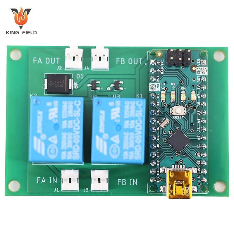
Through-Hole Assembly
As a PCBA manufacturer with over 20 years of professional experience , KING FIELD is committed to providing global customers with high-quality, highly reliable through-Hole Assembly solutions.
☑Precision welding is employed
☑ Soldering type : Lead-containing; Lead-free (RoHS compliant); Water-based solder paste
☑ Order quantity : 5 to 100,000 pieces
Description
What is through-hole PCB assembly?
Through-hole assembly is a PCB manufacturing process in which electronic components with leads /pins are inserted into pre-drilled holes in the board. These leads are then soldered to conductive pads or traces, forming a strong electrical and mechanical connection. Unlike surface mount technology (SMT), which places components directly on the board surface, through-hole components penetrate the board, thus ensuring greater stability under stress.
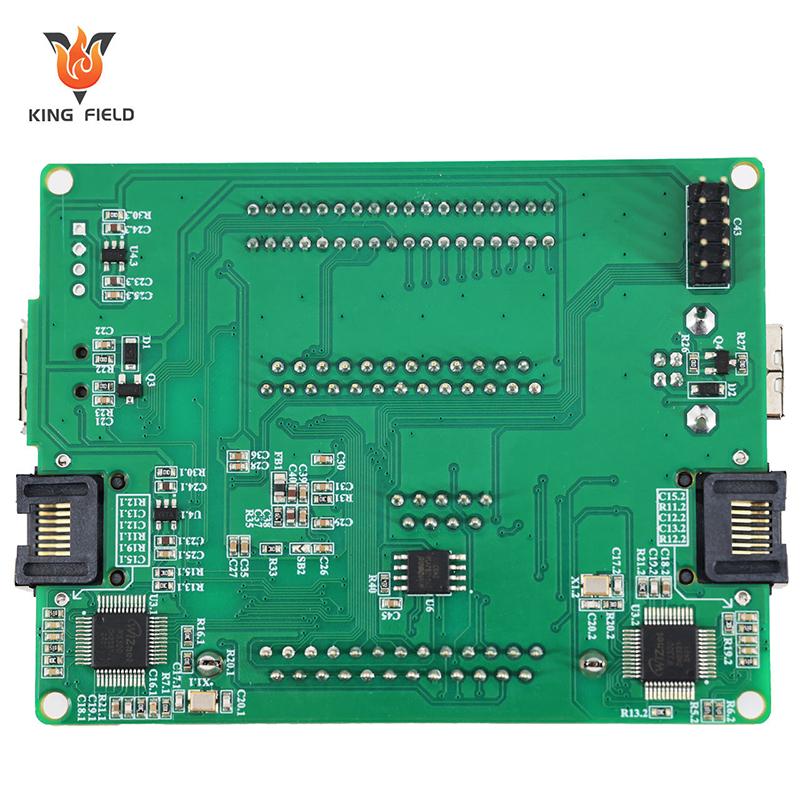
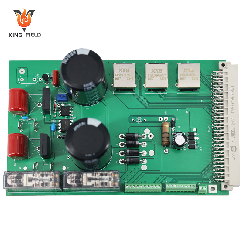
KING FIELD's through-hole PCB assembly capabilities
Minimum assembly component : 01005
Minimum BGA thickness: 0.3mm for rigid boards; 0.4mm for flexible boards;
Minimum precision lead size: 0.2mm
Component assembly accuracy: ±0.015mm
SMT capacity: 60,000,000 chips/day
Delivery time: 24 hours (express)
Component types : passive devices, minimum size 0201 (inch), chips with pitch as small as 0.38mm, BGA (0.2mm pitch), FPGA, LGA, DFN, QFN packages, and X-ray inspected.
Quality Inspection : AOI inspection; X-ray inspection; voltage testing; chip programming; ICT testing; functional testing
Features: High reliability , easy to operate manually , greater durability , lower manufacturing efficiency , durability , mechanical strength and durability , high power and high voltage capability , easy to assemble, repair and rework manually , reliability in harsh environments .
Why choose KING FIELD for through-hole PCB assembly?
20+ years of industry experience
- Founded in 2017, KING FIELD boasts a technical team with over 20 years of experience in printed circuit board design, possessing expertise in the complex structures and applications of flexible printed circuit boards.
- We have also built a complete manufacturing platform that integrates front-end R&D design, procurement of superior components, precision SMT placement, DIP insertion, complete machine assembly and full-function testing, which can quickly respond to your diverse order needs.
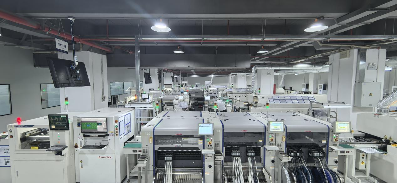
Factory rapid response
- The SMT factory supports medium to high-volume production and has strong capacity expansion capabilities , with a daily capacity of up to 60 million points.
- With 20 years of turnkey ODM/OEM experience , we provide one-stop PCB/ PCBA manufacturing services and can quickly respond to your diverse needs.
Quality assurance
- KING FIELD is equipped with a flying probe tester, 7 automated optical inspection (AOI) units, X-ray inspection, functional testing and other complete testing systems to achieve full-process quality control.
- In terms of quality control, our company has passed six major system certifications: IATF 16949, ISO 13485, ISO 9001, ISO 14001, ISO 45001, and QC 080000. We use a digital MES system for full traceability to ensure that every PCBA is of consistent quality.
After-sales service
KING FIELD offers a rare "1-year warranty + lifetime technical consultation" service. We promise that if a product has a non-human-caused quality problem, we will return or exchange it free of charge and bear the relevant logistics costs.
- The after-sales team's average response time is no more than 2 hours.
- Problem resolution rate exceeded 98%

FAQ
Q1 : What is your process for manufacturing through-hole PCBs?
KING FIELD : At KING FIELD, the manufacturing process for through-hole PCBs starts from the inner layer, then involves multi-layer lamination, precision drilling, copper plating of the hole walls , followed by outer layer circuitry and surface treatment, and finally testing before shipment.
Q2 : What are the technical challenges in the drilling process of your through-hole PCBs?
KING FIELD : The key challenges in our drilling process are ensuring that the hole walls are straight and smooth, dealing with the challenges posed by materials of different hardness, controlling the temperature and speed of the drill bit at all times, and avoiding the generation of burrs and residues.
Q3 : What is the principle of hole metallization?
KING FIELD : KING FIELD's hole metallization principle is to first deposit a thin layer of conductive copper on the insulating hole wall using chemical methods, and then thicken it through electroplating .
Q4 : What are the advantages and disadvantages of your wave soldering and manual soldering?
KING FIELD : Our wave soldering requires soldering the entire board at once, which is fast but not flexible enough; while our manual soldering can precisely handle each solder joint, which is flexible but inefficient. Therefore, more people are now choosing the compromise of selective wave soldering.
Q5 : What are some common quality problems during through-hole PCB manufacturing?
KING FIELD : The most common problems we encounter during through-hole PCB manufacturing are blocked holes, poor soldering, and board warping.