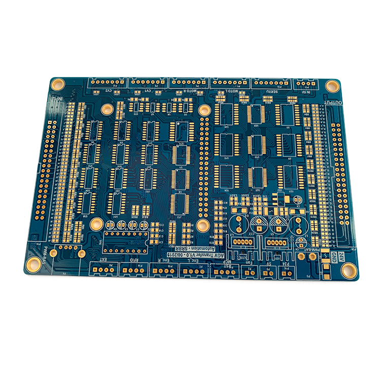
Superior Space and Weight Efficiency with HDI Rigid Flex PCB
HDI rigid flex PCB technology delivers substantial gains in physical footprint reduction by integrating what would traditionally be separate circuit boards, connectors, and cables into a single, cohesive structure. This consolidation translates directly into measurable benefits for weight-sensitive and space-critical applications—especially where reliability, miniaturization, and signal performance cannot be compromised.
Eliminating Connectors and Cables Reduces Volume by 40–60% vs. Rigid-Only Assemblies
The foundational advantage of HDI rigid flex PCBs lies in their consolidated architecture. By replacing discrete wire harnesses, board-to-board connectors, and associated mounting hardware with a unified interconnect solution, these designs reduce overall device volume by 40–60% compared to traditional rigid-only assemblies—data consistently validated across industry case studies from leading manufacturers. This dramatic space savings is essential for compact wearables, portable diagnostic sensors, and densely packed autonomous vehicle control units.
Integrated Architecture Lowers Mass and Improves MTBF—3.2× Reliability Gain (NASA GSFC Data)
Beyond size reduction, the seamless integration of rigid and flexible sections eliminates hundreds of potential failure points—including solder joints, crimped connectors, and interface mismatches—that are vulnerable to vibration, thermal cycling, and mechanical stress. NASA Goddard Space Flight Center’s 2023 reliability testing confirmed a 3.2× improvement in Mean Time Between Failures (MTBF) for HDI rigid flex architectures versus connector-dependent rigid alternatives. This proven reliability edge supports mission-critical deployments in satellites, implantable medical devices, and industrial robotic joints—where field failure is unacceptable.
Enhanced Signal Integrity and EMI Performance in HDI Rigid Flex PCB
Controlled Impedance Routing Across Rigid-Flex Transitions Enables Stable >5 GHz Operation
High-frequency signal integrity hinges on consistent impedance control—particularly at rigid-flex transitions, where material properties and layer stack-up geometry shift abruptly. HDI rigid flex PCBs meet this challenge through precision-engineered stack-ups: uniform dielectric thickness, tightly controlled trace widths, and laser-drilled microvias that replace disruptive through-holes at transition zones. Combined with embedded ground planes that provide low-inductance return paths, this design approach minimizes impedance discontinuities and signal reflections—enabling stable, low-jitter operation above 5 GHz. The result is robust high-speed data transmission in compact medical imaging systems, satellite transceivers, and 5G infrastructure modules.
Laser-Drilled Microvias and Embedded Ground Planes Reduce Crosstalk by Up to 70%
Dense routing in high-speed, multi-layer PCBs invites crosstalk—especially when signals cross between rigid and flex regions or traverse multiple layers via conventional vias. HDI rigid flex PCBs mitigate this through two synergistic features: laser-drilled microvias shorten vertical signal paths and reduce parallel coupling length, while embedded ground planes act as electromagnetic shields between active layers. Edge via stitching further contains radiated emissions. Together, these techniques lower near-field crosstalk by up to 70% compared to conventional rigid assemblies reliant on discrete connectors—delivering cleaner signal transmission and inherently lower EMI. This performance is critical for meeting Class III certification requirements in aerospace, defense, and life-critical medical electronics.
Proven Reliability and Miniaturization for Mission-Critical HDI Rigid Flex PCB Applications
HDI rigid flex PCB solutions deliver unparalleled reliability and miniaturization for industries where failure carries severe operational, regulatory, or human consequences. These advantages stem from structural integration—not just component-level optimization—enabling sophisticated functionality within constrained physical envelopes.
Medical: Implantable Devices Like Medtronic’s Cardiac Monitor (6L, 50μm lines, <0.3mm flex zones)
In implantable medical electronics, HDI rigid flex PCBs enable radical miniaturization without sacrificing safety or performance. Devices such as Medtronic’s next-generation cardiac monitors integrate six functional layers—including laser-drilled microvias and ultrathin flexible zones under 0.3 mm—into sub-centimeter form factors. Trace widths as narrow as 50 μm (45% finer than typical medical PCBs) maximize routing density, while seamless rigid-to-flex transitions eliminate vibration-prone connectors. These designs comply fully with IEC 60601-1 safety standards and achieve MTBF ratings exceeding 100,000 hours—validated using NASA GSFC reliability modeling frameworks.
Aerospace & Wearables: High-Growth Adoption Driven by SWaP-C Constraints and Class III Certification Needs
Aerospace and wearable electronics operate under stringent SWaP-C (Size, Weight, Power, and Cost) constraints—and increasingly, Class III certification mandates for flight-critical or life-sustaining functions. HDI rigid flex PCBs address both by replacing bulky, failure-prone connectorized assemblies with lightweight, monolithic circuits. Satellite communication modules now deploy 7+N+7 stacked microvia architectures to cut mass by up to 60% while preserving RF performance; radiation-hardened polyimide substrates ensure long-term survivability in orbit. Similarly, wearable health monitors leverage dynamic flex durability—withstanding over 100,000 bending cycles—while maintaining signal fidelity and regulatory compliance. This convergence of reliability, miniaturization, and electromagnetic resilience makes HDI rigid flex the de facto standard for next-generation mission-critical systems.
FAQ
What is an HDI rigid flex PCB?
HDI rigid flex PCBs combine high-density interconnect (HDI) capabilities with the structural flexibility of flexible circuits. They integrate both rigid and flexible sections into a single cohesive unit, enabling space and weight efficiency as well as improved reliability.
How do HDI rigid flex PCBs improve reliability compared to traditional rigid boards?
By eliminating separate connectors, solder joints, and crimped cables, HDI rigid flex PCBs reduce potential failure points caused by vibration, temperature cycling, and mechanical stress. NASA data shows a 3.2x Mean Time Between Failures (MTBF) improvement.
Which industries benefit most from HDI rigid flex PCB technology?
Industries such as aerospace, medical devices, wearable electronics, and automotive benefit greatly due to their need for miniaturization, reliability, and signal integrity in mission-critical applications.
How do these PCBs improve signal integrity?
HDI rigid flex PCBs offer controlled impedance routing, laser-drilled microvias, embedded ground planes, and edge via stitching to minimize signal interference and ensure stable performance at high frequencies.
What applications use HDI rigid flex PCBs?
HDI rigid flex PCBs are used in implantable medical devices, satellite communication modules, wearable health monitors, medical imaging systems, and autonomous vehicle control units, among others.