Quick Links
A Printed Circuit Board (PCB) is just one of among the most important innovations in contempoary electronic devices. If you have ever before used a wise tool, notebook computer, automobiles and truck dashboard, medical screen, Wi-Fi router, or clever home gizmo, you have presently depended upon a PCB without likewise considering it. In very easy terms, a PCB is the electronic motherboard that offers devices a secure framework for connecting and sustaining parts. It acts as the framework of essentially every electronic thing, which is why acknowledging what is a printed motherboard is so useful for designers, item designers, makers, students, and also interested consumers.
At its core, a PCB fixes a really practical concern: just how do you link lots of electronic get rid of each other in such a way that is tiny, reputable, and efficient? Prior to PCBs happened common, electronic gadgets were often created with point-to-point circuitry. That approach worked, however it was large, difficult to repair, and far less trusted. Today, a PCB uses copper traces, PCB layers, and a shielding substrate to produce exact electric courses. This makes the board not simply a physical support structure, yet likewise a controlled system for signal transmission, power circulation, and aspect intergration. To place it merely, the PCB is both a circuit service provider and an essential part of the device's feature.
The importance of PCBs has in fact simply boosted as digital tools have in fact diminished, faster, and more powerful. Modern gadgets need more performance in a lot less location, and that has actually pushed the PCB market toward advanced alternatives such as multi-layer PCB designs, HDI PCB advancement, versatile PCB designs, and rigid-flex PCB frameworks. These growths aid sustain every little thing from small wearable modern-day innovation to high-speed servers and safety-critical automotive systems. According to sector patterns, the PCB manufacturing and PCB establishing market remains to expand due to the fact that every new generation of electronic devices requires much better PCB design, far much better PCB construction, and far better automation.
Printed circuit boards are made use of to attach, assistance, and control electronic components in nearly every sort of digital device. If a product uses electric power in an orderly technique, there is commongly a PCB inside it. The specific task of the board relies upon the device, however the essential function coincides: develop trustworthy electric paths for signals and power. That is why the search inquiry what are published motherboard utilized for is so typical. PCBs are not used for just one inudstry or one sort of product-- they are utilized anywhere.
In customer products, PCBs aid control displays, sensors, cordless communication, audio, payment, and processing. In commercial systems, they handle automation, device control, and power circulation. In medical gadgets, they sustain life-saving tracking and analysis tools. In autos, they pwoer control board, control components, safety and security systems, and paid announcement. In aerospace and protection, PCBs are made use of in high-reliability systems that need to accomplish under resonance, warm, and stress. The same core innovation is gotten used to every atmosphere by transforming the PCB products, PCB layers, and PCB setting up process.
|
Industry |
Common PCB Applications |
|
Consumer electronics |
Smartphones, laptops, tablets, Televisions, smart devices |
|
Automotive |
Dashboard screen screens, ECUs, ADAS systems, paid announcement, battery control |
|
Medical |
Heart presents, blend pumps, imaging systems, implantable tools |
|
Industrial |
PLCs, robots, electrical motor controllers, producing facility automation tools |
|
Telecom |
Routers, servers, 5G components, network buttons |
|
Aerospace & defense |
Navigation systems, satellites, avionics, unbiased electronic gadgets |
PCBs implement a number of critical functions at the same time:
Attach electronic parts
Path signals in between chips and parts
Disperse electric power
Help mechanical security
Lower sound and disruption
Boost signal stability
Keep circuits arranged and mobile
Right here are some of the most typical PCB applications you will see in the real life:
Smartphone PCB: Cares for handling, battery charging, camera control, cordless communication, and present links
Computer system motherboard: Feature as the major platform for CPU, memory, storage space, GPU, and development ports
Automotive PCB: Supports engine control, safety and safety and security features, lighting, sensing devices, and commercial systems
Clinical tool PCB: Enables exact surveillance, control, and communication in treatment tools
Wearable modern technology PCB: Powers small smartwatches, fitness bands, and and health and health sensors
Industrial PCB applications: Control equipment, manufacturing center automation, and power electronic devices systems
PCBs are common due to the truth that they incorporate:
Portable measurement
High integrity
Easy mass production
Low blunder rates
Solid electric efficiency
Personalized layout flexibility
This makes them excellent for both straightforward and very progressed digital gadgets. Whether a product needs a tiny single-sided board or a complex multi-layer PCB, the very same fundamental concept works.
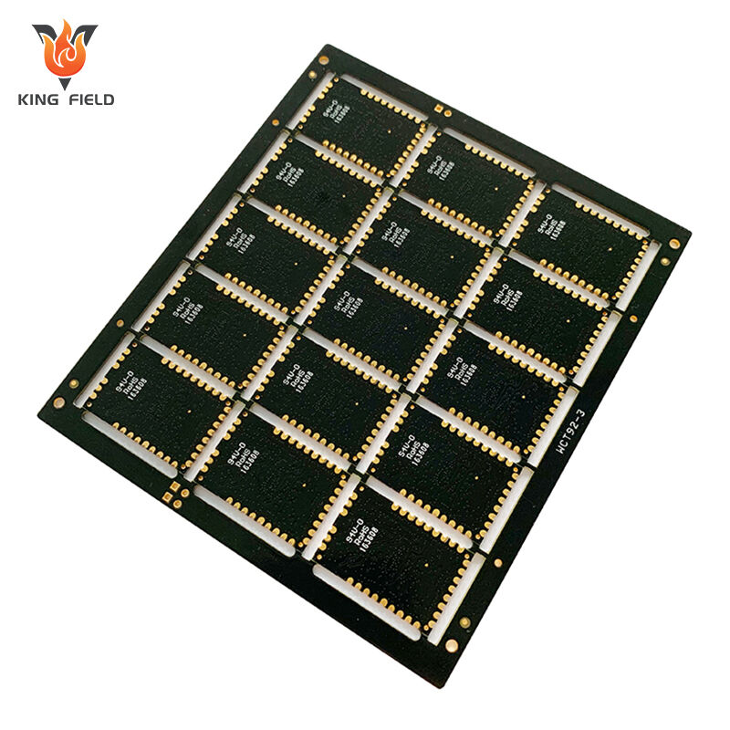
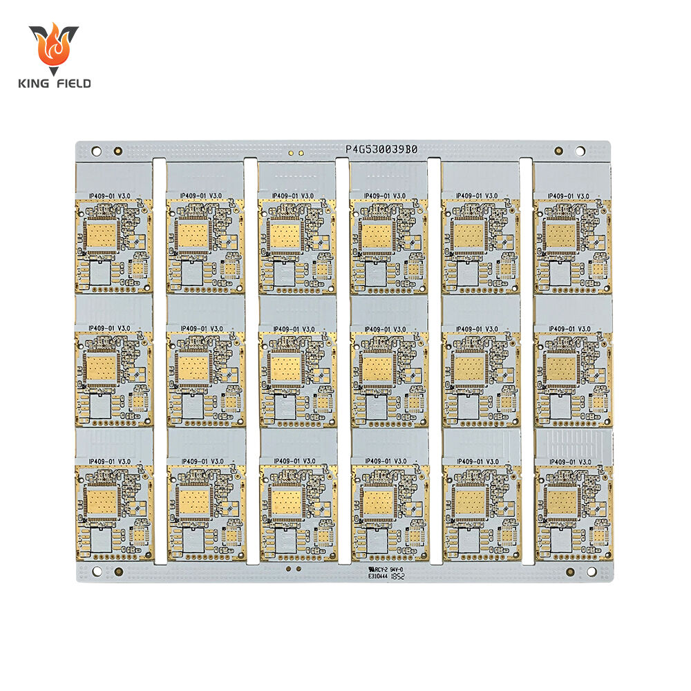
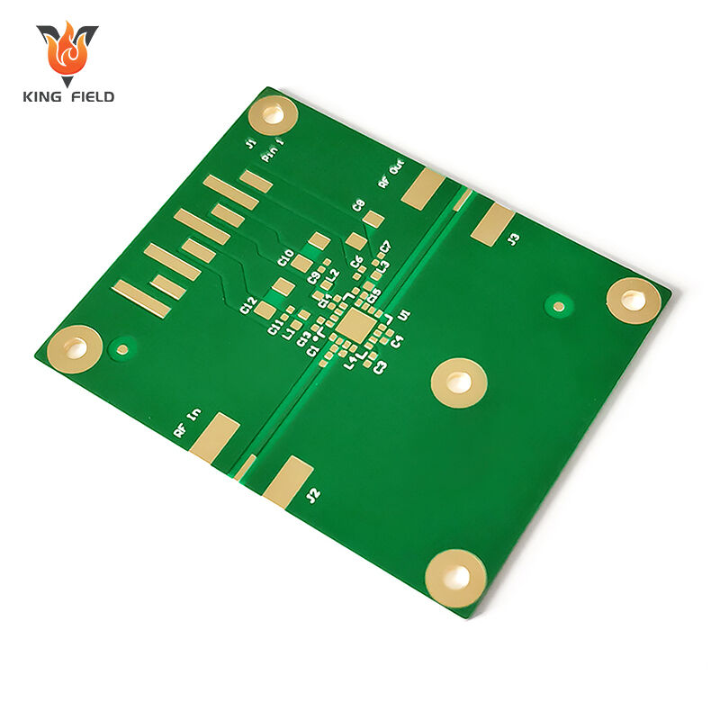
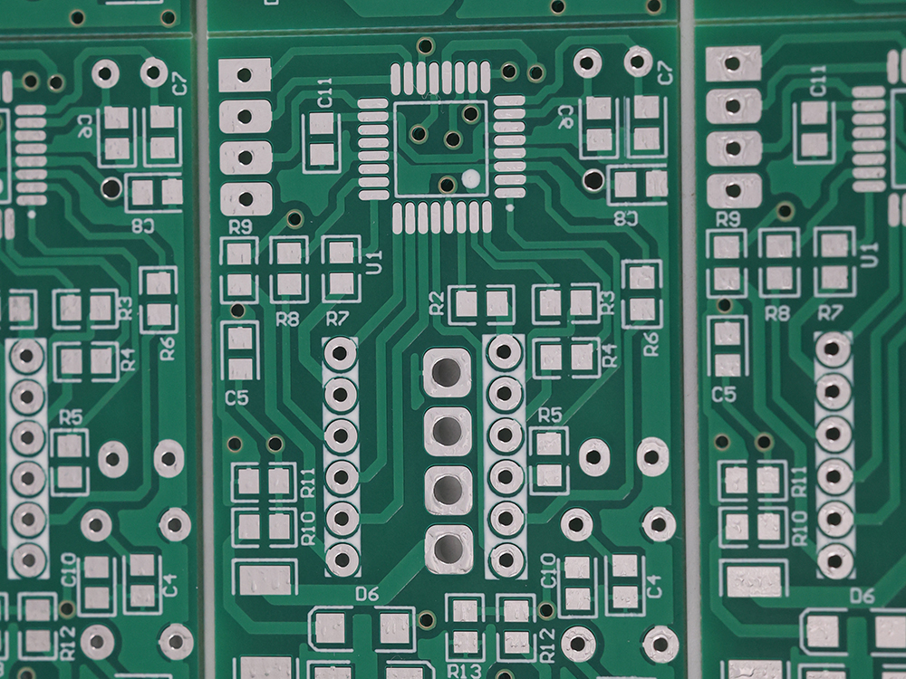
Recognizing PCB framework and PCB products is among the most reliable means to comprehend just how a board genuinely functions. A PCB is not simply a degree item of green plastic. It is a diligently split structure established from products that need to take care of electric performance, cozy, mechanical anxiety, and creating treatments. The combination of substrate, copper, product, solder mask, and silkscreen develops a protected platform for digital components and conductive paths.
Among the most typical base material is FR-4 product, a fiberglass epoxy laminate. FR-4 projects considering that it offers terrific insulation, solid mechanical security, and an affordable expense. On top of that base, manufacturers add copper aluminum foil layers, which come to be the PCB traces and copper planes after etching. A solder mask covers the board and guards the copper from oxidation and unintended short circuits. Finally, the silkscreen layer consists of tags, recommendation designators, logos, and establishing markings.
|
Layer / Material |
Purpose |
|
Board substrate |
Provides mechanical assistance and insulation |
|
FR-4 material |
Common fiberglass epoxy laminate base |
|
Copper foil |
Forms conductive pathways |
|
Prepreg resin |
Bonds layers together in multilayer boards |
|
Solder mask |
Protects copper from shorts and damages |
|
Silkscreen layer |
Adds tags, indicators, and component marks |
A PCB stackup is the arrangement of copper and insulating layers inside the board. In a simple board, the stackup might simply include a number of layers. In a multi-layer PCB, the stackup can contain great deals of signal layers, ground airplanes, and power airplanes. The approach these layers are ready influences effectiveness, electro-magnetic disturbance decrease, thermal management, and directing effectiveness.
The PCB traces are the slim copper lines that bring signals and present. Their size and density issue because they impact resistance, existing capability, and heat accumulation. The ground airplanes help in reducing electrical noise, while the power aircrafts distribute power similarly accross the board. With each other, these components establish an extra steady and foreseeable circut setting.
Different tools need various products. As an example:
Customer electronic gadgets frequently utilize FR-4 due to the fact that it is spending plan friendly and reputable
High-speed or high-frequency designs may require low-loss products
High-power systems could require hefty copper or metal core building
Versatile digital gadgets require polymer-based products that can bend
|
Performance Factor |
Why It Matters |
|
Heat resistance |
Prevents problems from high operating temperature level levels |
|
Resonance resistance |
Important in autos, plane, and business tools |
|
Wetness resistance |
Helps protect against damage and failure |
|
Signal integrity |
Maintains neat, exact electrical signals |
|
PCB durability |
Extends product life-span |
|
Thermal management |
Helps maintain components within risk-free temperature degree limits |
A cellphone board takes advantage of a compact PCB stackup with several layers due to the fact that it needs thick directing, reduced audio, and reliable effectiveness in a really little space. A power inverter PCB, on the other hand, might make use of thicker copper and even more powerfull thermal materials because of the reality that it should take care of far more existing and warmth. This is why PCB items are not one-size-fits-all. The style must match the application.
A PCB works by producing controlled electrical web links in between electronic elements through copper paths, pads, and vias. When power is connected to the board, the copper traces lead existing from one part of the circuit to one more in a precise method. The board does not "believe" by itself, yet it supplies the structure that allows integrated circuits, picking up systems, microcontrollers, memory chips, and other parts to interact properly. Without this framework, contemporary board-level digital gadgets would absolutely be additionally unpleasant, too undependable, and as well difficult to generate at range.
The most essencial idea behind precisely how a PCB functions is that electricity abides by the conductive courses made right into the board. These courses are not approximate. They are created making use of PCB format devices, style policies, and signal analysis to ensure each trace does its work. Some traces lug info signals, some lug power, and some assistance specify grounding and protecting actions. Vias link one layer to another, while ports enable the board engage with external parts or numerous other boards.
A copper trace is basically a released cord. It is a slim strip of copper etched right into a board to relocate present or signals between components. Trace size, trace thickness, and spacing are very important. A trace that is also narrow might get also warm or create excessive resistance. A trace that is also near an extra signal might activate sound or crosstalk. That is why PCB guiding need to adhere to clear design policies.
|
Via Type |
Description |
Use |
|
Through-hole vias |
Go via the full board thickness |
Common in lots of boards |
|
Blind vias |
Connect external layer to internal layer |
Save area in thick styles |
|
Concealed vias |
Connect internal layers only |
Used in ingenious multilayer boards |
|
Microvias |
Very small vias for HDI designs |
High-density adjoin boards |
PCBs frequently connect to numerous other parts of the system taking advantage of:
Board-to-board adapters
Wire-to-board adapters
Input/output adapters
Bow adapters
Side adapters
These enable the PCB to function as part of a bigger digital system as opposed to a standalone board.
When a tool is activated, the PCB assists program power to the appropriate parts. The microcontroller might send out guidelines, sensing units might send out information, and memory chips may keep information. The traces bring these signals across the board. Ground airplanes aid preserve the system. Power planes disperse existing similarly. In high-speed formats, insusceptibility control is taken advantage of to preserve signal high quality.
Parts can be attached to the board in two significant ways:
Surface Mount Technology (SMT): Parts are put straight externally
Through-Hole Modern Technology (THT): Leads travel through openings in the board
SMT is perfect for miniaturized digital gadgets and computerized manufacturing. THT is still valuable when mechanical stamina concerns, such as for ports or power components.
A great deal of PCBs are made from FR-4 material, which is a fiberglass epoxy laminate. They in addition contain copper light weight aluminum foil, product layers, solder mask, and silkscreen. Specialized boards might make use of polyimide, ceramic, lightweight aluminum, or various other items depending upon the application.
Yes, you can establish a PCB in your home using EDA devices or PCB design software program application. Various beginners start with easy boards and after that send the style to a maker for PCB prototyping. Home design is really typical for hobby electronic devices, deep-rooted systems, and discovering work.
A PCB must normally be cleaned with isopropyl alcohol and a soft brush or lint-free towel. You should remain clear of harsh chemicals, excess moisture, and unnecessary pressure. If the board is powered or linked to numerous other parts, ensure is securely separated initially.
A PCB itself is neither air conditioning neither DC. It is a board that brings circuits. The circuits on the board may make use of a/c, DC, or both depending upon the device. As an exemple, a power supply area might transform a/c to DC, while different other circuits run simply on DC.
The time depends on style intricacy, components accessibility, and volume.
Version boards: normally 2-- 5 days
Production runs: often 1-- 3 weeks
Decision
Printed circuit boards are the foundation of contemporary electronic gadgets. They make it possible to develop small, reliable, and high-performance tools by incorporating mechanical aid with arranged electric courses. Whether the item is a smart device, automobile controller, clinical screen, router, or industrial maker, the PCB is what enables the electronic elements to collaborate as a system.
The largest benefit of PCBs is their adaptability. A basic single-sided PCB can sustain a standard tool, while a multi-layer PCB, adaptable PCB, or rigid-flex PCB can power advanced innovations with requiring area, rate, and honesty needs. As digital tools remain to lessen and become more smart, the need for much better PCB manufacturing, much better PCB design, and much better PCB assembly will just grow.
 Hot News
2026-05-27
2026-05-25
2026-05-21
2026-05-06
2026-04-18
2026-04-17
2026-04-13
2026-04-12