BGA Assembly Delivers Unmatched Interconnect Density and Miniaturization
How BGA Assembly Enables Higher I/O Count in Smaller Footprints
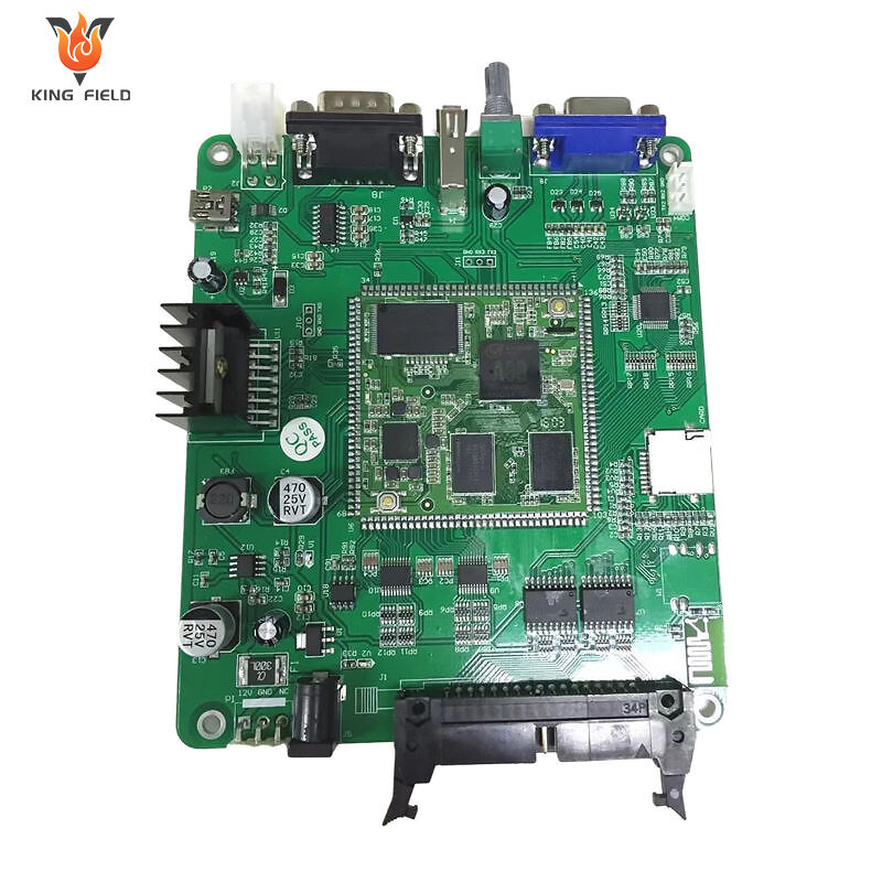
BGA assembly leverages a full area-array of solder balls beneath the package, enabling hundreds to thousands of interconnects within a compact footprint. Unlike peripheral-lead packages such as QFPs—which are limited by edge-based pin spacing—the grid layout maximizes connection density without increasing package size. This architecture directly supports electronics miniaturization: smartphones, wearables, and high-performance computing modules rely on BGA to integrate more functionality into smaller boards. Fine-pitch micro-BGA variants further extend this capability, supporting ultra-high pin counts for advanced processors and memory devices. The resulting interconnect density also reduces PCB layer count by consolidating signals into a small area, lowering overall design complexity.
Thermal and Electrical Benefits of Area-Array Interconnection
The area-array configuration delivers distinct thermal and electrical advantages. Each solder ball serves as a conductive thermal path, distributing heat from the IC to the PCB more efficiently than perimeter-based packages—lowering operating temperatures and improving long-term reliability. Electrically, the short, symmetrical connections reduce parasitic inductance and resistance, enhancing signal integrity for high-speed data transmission. Uniform ball placement also supports low-inductance power and ground planes, minimizing voltage droop during dynamic loads. These benefits make BGA assembly essential for applications demanding both dense routing and robust performance—such as networking infrastructure and GPU modules.
Key BGA Assembly Routing and Layout Challenges in High-Density PCBs
Escape Routing Constraints and Optimal Layer Stackup Planning
Routing signals out of a fine-pitch BGA is among the most demanding tasks in high-density PCB design. Tight ball pitch severely limits trace escape space, requiring deliberate layer stackup planning. Outer layers typically handle initial fanout with short traces, while inner layers manage longer routes. The total layer count must balance routing feasibility against cost—too few layers cause congestion and routing failure; too many increase fabrication expense and signal loss. Maintaining consistent impedance across signal layers adds another constraint. A proven strategy is to place dedicated ground and power planes adjacent to high-speed signal layers, which improves return path continuity and suppresses crosstalk. Without optimized stackup planning, escape bottlenecks can trigger signal degradation and manufacturing defects.
Vias-in-Pad vs. Microvias: Trade-offs for Signal Integrity and Manufacturability
Designers choosing between vias-in-pad and microvias must weigh performance, space, cost, and reliability.
| Feature | Vias-in-Pad | Microvias |
|---|---|---|
| Signal Integrity | Superior for high-speed designs due to minimal stub length | Good performance, though longer stubs may degrade GHz-range signals |
| Space Utilization | Consumes pad real estate, limiting adjacent routing channels | Enables routing directly under the package, maximizing board utilization |
| Manufacturing Cost | Lower cost, but requires reliable plugging and planarization | Higher cost due to laser drilling and sequential lamination processes |
| Reliability | Risk of solder voiding if fill quality is inconsistent | Highly reliable when used within IPC-recommended layer limits |
For ultra-dense BGA assembly, microvias offer greater routing flexibility and signal fidelity—but at increased cost and process complexity. Vias-in-pad remain a practical, cost-effective solution when paired with proven fill and plating controls. The final choice depends on signal speed requirements, layer budget, and production constraints.
Ensuring Signal Integrity Through BGA Assembly Best Practices
Impedance Control, Crosstalk Mitigation, and Grounding Strategies
Maintaining signal integrity in high-density BGA designs hinges on disciplined impedance control. Trace width, spacing, and dielectric thickness must be precisely calculated to achieve target characteristic impedance—typically 50 Ω single-ended or 100 Ω differential. Adjacent reference planes ensure continuous return paths and minimize loop inductance. To mitigate crosstalk, designers limit parallel trace lengths and increase spacing between critical high-speed nets. A solid ground plane—reinforced with ground-stitching vias around BGA periphery signals—suppresses electromagnetic interference and stabilizes the power delivery network (PDN). Applying these best practices early in BGA assembly ensures clean, reliable high-frequency signaling and prevents data corruption or system-level failures.
BGA Assembly Reliability: From Placement to Rework
Critical Process Controls for Accurate Placement, Reflow, and AOI Inspection
High-yield BGA assembly relies on tightly controlled processes at every stage. Automated placement systems achieve sub-25µm positional accuracy for microscopic BGAs, ensuring correct orientation before soldering. During reflow, multi-zone ovens maintain peak temperatures at 245°C (±5°C) for lead-free alloys, using gradual ramp profiles to minimize thermal stress and keep solder voiding below 75%—in compliance with IPC-7095 guidelines. Post-reflow Automated Optical Inspection (AOI) validates results with high-resolution imaging, detecting micro-cracks, insufficient fill, and misalignment to 99.92% accuracy per IPC-A-610 Class 3 standards. Regular calibration maintains traceability for solder sphere coplanarity measurements—ensuring deviations stay under 150µm. Together, precision placement robotics, thermally optimized reflow profiling, and multi-spectral AOI form a robust defect-interception framework that significantly reduces field failures.
FAQs
1. What is BGA assembly, and why is it important?
BGA (Ball Grid Array) assembly is a packaging technology used to provide a high density of interconnections within compact spaces. It enables miniaturization and improved performance in devices like smartphones, wearables, and GPUs.
2. How does a BGA package support thermal and electrical performance?
The area-array solder balls in a BGA package distribute heat and reduce parasitic electrical resistance and inductance, improving overall thermal and signal integrity.
3. What are the key challenges in routing BGA assemblies?
Challenges include tight routing space due to fine pitch, impedance control, and optimizing layer stackup to avoid signal degradation and PCB congestion.
4. When should I use vias-in-pad versus microvias?
Vias-in-pad are cost-effective and reliable when proper filling is implemented, while microvias are preferred for ultra-high-density designs, despite their higher costs and complexity.
5. What practices ensure signal integrity in BGA designs?
Precise impedance control, crosstalk mitigation, and maintaining continuous grounding using ground-stitching vias are key practices to ensure robust signal integrity.
6. How does Automated Optical Inspection (AOI) improve BGA assembly reliability?
AOI systems detect defects like micro-cracks and solder misalignments with high precision, ensuring high assembly quality and preventing failures in the final product.
Table of Contents
- BGA Assembly Delivers Unmatched Interconnect Density and Miniaturization
- Key BGA Assembly Routing and Layout Challenges in High-Density PCBs
- Ensuring Signal Integrity Through BGA Assembly Best Practices
- BGA Assembly Reliability: From Placement to Rework
-
FAQs
- 1. What is BGA assembly, and why is it important?
- 2. How does a BGA package support thermal and electrical performance?
- 3. What are the key challenges in routing BGA assemblies?
- 4. When should I use vias-in-pad versus microvias?
- 5. What practices ensure signal integrity in BGA designs?
- 6. How does Automated Optical Inspection (AOI) improve BGA assembly reliability?

