Before you can with self-confidence recognize elements on a PCB, you must discover specifically how to review schematics-- the "plans" made use of by engineers in format, manufacturing, and dealing with.
Rather than revealing the physical locations of each component, it utilizes common digital schematic icons to visualize connections and attributes. This abstraction is your trick to understanding just how any type of sort of circuit functions, regardless of its measurement or application.
Universal language: Schematics allow you "have a look at" a circuit regardless of supplier, trademark name, or language.
Faster troubleshooting: Recognize issues by following signal training courses from resource to heaps.
Much less difficult style and upgrades: Modification or upgrade existing styles with a lot less uncertainty.
Resistor & variable resistor (potentiometer, thermistor, varistor).
Capacitor (polarized, non-polarized, trimmer).
Inductor, transformer.
Semiconductors: diodes, transistors, ICs.
Power and ground: DC source, a/c source, ground (earth), fuse, battery.
A finest method for checking out motherboard and schematics is to start with the resource of power. This is normally the beginning indicate seek both repairing and understanding a new style.
Common Power Source Symbols & Their Meanings
|
Symbol
|
Schematic Name
|
Description
|
|
DC Symbol
|
V+/ Vcc/ Vdd
|
Direct present voltage resource
|
|
Cooling Icon
|
~ V
|
Alternating present voltage
|
|
Battery Symbol
|
Long-short-short-long
|
Indicates collection battery cells
|
|
Ground Symbol
|
Earth/common
|
Return program for existing, important reference
|
|
Fuse Symbol
|
Wire withh bar or zigzag
|
Overcurrent protection
|
|
Transformer
|
Coupled coils (in some cases dots, lines, or bars)
|
Changes voltage, isolates
|
|
Solar Cell
|
Battery with arrows
|
Alternative source of power
|
|
Managed Source
|
Arrow + box
|
Indicates variable/powered resource
|
Power Source Trace & Connections
Trace Joint: Disclosed as a dot or round; implies authentic link.
Trace Crossing (Cable Crossover): Lines that go across without dot-- suggests no link (simply overlooks).
Net Junctions: Made use of to acknowledge nodes, voltage rails.
Study: When power supply fixing a malfunctioning PCB, professionals always initially confirm the existence of power at each phase-- frome DC input to plan, to result rails-- using schematic resource of power signs as their review.
Acknowledging these power location symbols and beginning your circuit analysis from the source of power can promptly disclose issues like blown integrates, failed diodes, or open circuit traces, and informs you precisely how the remainder of the parts are being powered and shielded.
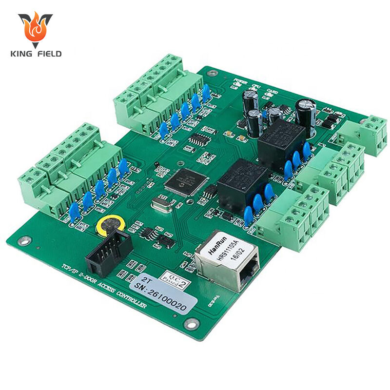
How to Identify Components on a Circuit Board (Step-by-Step)
Components and their functions and types of circuit board components
Identifying parts on a PCB incorporates understanding, cautious assessment, and a sensible strategy. Below's a sensible, thorough strategy that professionals take advantage of:.
Step 1: Determine the Board’s Purpose
Check out any kind of kind of board markings, silkscreen notes, or design numbers.
Search for a block representation, application recap, or BOM (costs of products) if readily available.
Instance: "DC Motor Controller", "Power Supply", "WiFi Module".
Step 2: Inspect Passive Components
Resistors: Determine by physique (axial, SMD), shade code (bands), or numbers for SMDs.
Capacitors: Ceramic are small/beige; electrolytic are cylinder-shaped; note polarity (+/-) marks.
Step 3: Carefully Evaluate Integrated Circuits (ICs)
Review IC element numbers and lookup their datasheets for pin features.
Check bundle layout: DIP (dual in-line), SOIC (little summary), QFP (quad degree), BGA (ball grid).
Find pin 1 (dot, notch, beveled side for positioning).
Step 4: Identify Other Discrete Components
Diodes: Stripe marks cathode -LRB----RRB-.
Transistors: BJT (3 legs: B, C, E), FET (G, D, S). Try to find component numbers.
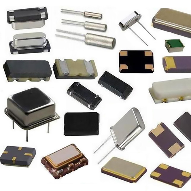
Crystals: Marked by frequency.
Connectors/Relays: Examine tags and pinouts.
Step 5: Reference Designators and Schematics
Use silkscreen letters and numbers to match the component to the schematic indication:.
R: resistor, C: capacitor, L: inductor, D: diode, Q: transistor, U: IC, F: fuse, J: adapter, T: transformer, and more.
Step 6: Research Unknown Components
Browse part numbers, strategy codes, or visual attributes on producer sites or conversation online forums.
Usage datasheets, area resources, or perhaps reverse photo seek unknown chips or strategies.
PCB Components Identification Techniques
Finding unknown or uncertain elements requires a mix of physical examination, measurement, and documents abilities.
Visual Inspection & Markings
When it refers to PCB parts acknowledgment, absolutely nothing defeats a thorough visual assessment. Begin by looking for manufacturer markings, distinctive codes, and silkscreen designators. The majority of SMD (surface location gizmo) elements are little-- utilizing a magnifier or a straightforward jewelry expert's loupe is essential. Some contemporary designers even take advantage of smart device camera or electronic microscopes to focus on markings that are almost unseen to the nude eye.
Secret visual tips:
Axial components (resistors, through-hole diodes): Search for colored bands (resistor shade code) or a red stripe (diodes) to indicate positioning.
Capacitors: Generally marked with worth or voltage; electrolytics have a clear polarity red stripe.
ICs & Semiconductors: Element numbers and manufacturer logo designs are printed on the top. Recommendation datasheets for pinouts and functions.
SMD codes: Some SMD aspects have cryptic alphanumeric codes. On the web SMD codebooks or supplier datasheets can assist decipher these.
Polarity pens: Search for a line, dot, bevel, or +/ − icon for polarized devices.
Measuring Tools
Basic dimensions can clear lots of uncertainties. Below's how you use your examination tools for identifying digital elements on a circuit board:.
Multimeter Connection Examination Take advantage of the conection setting to look for web links in between traces or accross integrates, along with for standard resistor worth examination.
Component Measurement (Resistance/Capacitance/Inductance): Some multimeters can gauge easy parts straight, also in-circuit (with accuracy cautions).
Diode Exam Setting: Examine forward voltage of diodes, LEDs, and also identify which lead is the anode or cathode.
Transistor Testing: Probe for BJT leg identification (base, debt collection agency, emitter), or FET (gateway, drain, resource) utilizing diode exam.
Schematic Cross-Reference
A schematic diagram is extremely practical for element recognition, particularly during PCB repair service, reverse engineering, or setting up confirmation.
Trace nets on the board: Silkscreen, or PCB design software application such as Cadence OrCAD, commonly labels webs and reference designators that correspond straight to the schematic.
Check the BOM (Bill of Products): If available, the BOM notes each designator along with the accurate component kind, worth, and supplier code for much less complicated sourcing.
Visual-Schematic Matching: Compare unique silkscreen kinds (rectangular shapes for dip ICs, small circles for test factors, polygons for pads) with the arranged schematic.
Additional Identification Aids
Recommendation tables or posters: Save time by maintaining a printout/chart of resistor shade codes, capacitor mark conventions, and regular schematic indications.
On the internet tools and applications: There are mobile applications for scanning resistor color codes, barcodes, or perhaps recognizing element lays out frome photos.
Advanced Identification: Polarized and Oriented Components
In PCB establishing (PCBA) and repair service, right positioning of parts is mission-critical, particularly for polarized parts. Stopping working to respect polarity can mess up components immediately.
Identifying Polarized Parts
Electrolytic capacitors: A lot of have a red stripe on the body with a minus indicator. The extensive lead is generally positive.
Tantalum capacitors: Usually, a '+' on the situation notes the positive side.
Diodes and LEDs: Red stripe or bar = cathode (−). The anode is typically kept in mind with a longer lead.
Integrated Circuits (ICs): Try to find a dot or little notch at one end-- this is pin 1. The alignment is vital for all ICs.
Transistors (BJT, MOSFET, JFET): Datasheets offer pin plans; on TO-92 plan, looking at the level side: left = Emitter, middle = Base, right = Enthusiast (for a number of BJTs, yet constantly inspect).
Pin 1 and Package Orientation
On QFP and SOP bundles, a dot or chamfered side signals pin 1. This is very important both for creating new boards and changing ICs during repair work service.
Silkscreen & Assembly Hints
Modern PCBs typically publish polarity indicators:.
'+' and '--' near part outlines.
Square pad: On a number of PCBs, the square solder pad marks pin 1 for ICs or the favorable pad for capacitors/diodes.
Arrowheads, notches, or dots: Help with manual/visual positioning.
Technique Takeaways:
Frequently triple-check for polarity/position prior to soldering.
Usage datasheets and silkscreen markings to confirm.
For vague scenarios, talk to the schematic or maker instructions.
Importance of Component Identification in PCB Assembly & Repair
The worth of precise PCB aspects recognition can not be overemphasized in digital tools manufacturing and servicing.
Why Identification Matters
Prevents Establishing Mistakes: Soldering the inaccurate element (inaccurate worth, or turned around polarity) can create destructive tool failing-- occasionally additionally harmful outcomes.
Speeds Up Troubleshooting: Comprehending just how to identify passive and energised components, and swiftly area malfunctioning systems, considerably minimizes fixing time.
Makes It Possible For Reverse Layout: For obsolete electronics (vintage repair solution) or inexpensive analysis, recognizing just exactly how to assess motherboard and establish components is irreplaceable.
Makes Sure Thing Premium & Conformity: Proper part positioning is crucial for passing electrical tests (ICT/FCT), RoHS/UL/ISO qualification, and regulative examination.
Help in Upgrades: Exchanging out an op-amp for a higher-performance variant, or retrofitting boosted filters, is just practical if you have actually accurately recognized the initial elements and their specifications.
Real-World Example
A telecommunications maker was dropping hundreds of bucks over stopped working items returned from the area. A root-cause evaluation exposed that motorists were misunderstanding the element placement for a polarized input diode (stripe → anode instead of cathode). When an increased silkscreen and establishing list were accepted, location failures stopped by 92%.
FAQs: Reading PCBs, Schematics, and Identifying Components1. What do the letters 'R', 'C', 'L', 'D', 'Q', and 'U' indicate on PCBs? They're called reference designators-- shorthand for element kinds:.
R: resistor.
C: capacitor.
L: inductor.
D: diode.
Q: transistor.
U (or IC): integrated circuit.
2. Just how do I tell the difference in between passive and energised aspects?
Easy components (resistors, capacitors, inductors) do not multiply or produce power; they just take in, keep, or launch it.
Energetic parts (transistors, op-amps, ICs, diodes) can multiply, switch, or control present flow.
3. Specifically just how do I acknowledge polarized capacitors on a PCB?
Look for a stripe noting, a '+' icon, or a long/short lead difference. The silkscreen typically has a '+' sign for the positive pin.
4. What are SMD and through-hole components?
Through-hole: Get rid of leads place by means of openings and soldered on behind-- durable, however bigger.
SMD (Surface Area Mount): Placed directly onto the PCB's surface area-- little, common in modern digital gadgets.
5. Where's pin 1 on an IC bundle?
Pin 1 is generally noted by a dot, notch, or chamfered corner. Examine the datasheet and confirm with the board's silkscreen.
 Hot News