Quick Links
A PCB trace is among the most indispensable parts of a printed circuit card, yet it is frequently disregarded by newbies. In fundamental terms, a trace is a copper trace or conductive copper course that lugs electrical present in between electronic components. Whenever a signal relocates from one chip to an additional, or power streams from a port to a gizmo, it normally travels via a PCB conductor. That recommends the trace is not merely a line on a board. It is the structure of PCB electric circuitry, PCB directing, and complete board feature. Without proper traces, also the best-designed circuit will certainly stop working to function precisely.
The reason PCB trace design matters a lot is that traces do greater than affix points on a board. They in addition influence PCB electric efficiency, signal stability, power circulation, voltage decrease, and heat dissipation. A trace that is too slim might obtain also warm or thaw. A trace that is too lengthy might develop resistance and slow-moving signal activity. A trace that is incorrectly directed could boost crosstalk, electromagnetic disruption, or signal depiction. Basically, the top quality of a PCB trace can determine whether a product does smoothly or stops working under tons.
This is why designers pay attention to PCB trace size, PCB trace thickness, and PCB trace existing very early in the style process. These aspects are not visual. They are style selections that affect safety, performance, and manufacturability. For example, a high-current electric motor vehicle driver board needs much broader traces than a tiny picking up device board. A high-speed digital board could require mindful trace spacing and resistance control. A flexible board might need different trace policies than an inflexible FR-4 board. The best choices rely on the circuit, the items, and the last application.
Understanding PCB trace width estimation and PCB trace resistance is useful for both newbies and skilled developers. Newbies commonly focus on element positioning and schematic links, yet the trace design is what changes the format into a useful physical item. Experienced engineers comprehend that trace style influences whatever from PCB overheating to PCB board stability. If you are developing a model, producing automation, or managing PCB construction and PCB establishing, trace competence is very important.
Below are several of the most significant factors map format concerns:
Existing lugging ability The trace should firmly manage the current without overheating.
Voltage security Lengthy or slim traces can produce unwanted voltage loss.
Signal excellent quality Poor sending can reduce signal honesty and boost noise.
Thermal performance Thin traces can act like powerlessness throughout high existing blood circulation.
Production success Good trace layout improves PCB manufacturability and reduces the opportunity of construction concerns.
Consider 2 PCB traces bring the similar existing. One trace is wide and short. The various other is slim and lengthy. The slim trace has even more resistance, so it heats up a lot even more and drops much more voltage along the roadway. Gradually, that can cause falling short. The vast trace, on the other hand, runs cooler and carries out better. This is why PCB trace sizing is so essential in PCB engineering and electronic design.
A little PCB version for an IoT device worked well throughout bench screening, yet failed after being placed in a warmer system. The difficulty was not the chip or the firmware. The issue was that the power trace was too narrow for the real operating current. As the board warmed up, the trace temperature rose, the resistance boosted, and the voltage went down below the levle needed by the sensor. A fundamental trace redesign resolved the trouble. This is a common circumstances of why trace sizing can not be taken care of as a second thought.
Good PCB design is not practically ideal components onto a board. It is about producing trusted electric paths that function under real operating problems. That indicates selecting the excellent trace geometry, using appropriate PCB transferring, and book-keeping for PCB thermal management. It furthermore suggests comprehending just how PCB services relate to the physical board. If you recognize simply exactly how present flows, simply exactly how resistance develops, and specifically just how warmth spreads out throughout copper, you can make much more powerful and much more trustworthy boards.
A PCB trace is more than an easy copper line. In modern-day PCB design, it is the actual course that permits power, details, and control signals to cross the board. Traces link electronic components such as ICs, resistors, capacitors, noticing units, ports, and power gizmos, making the circuit physically and electrically useful. Because sensation, traces are the real "roadways" of the board. Without them, a schematic would definitely stay just a principle in theory. With them, the design comes to be a working printed motherboard.
In today's electronics, traces need to do a lot more than lug existing. They need to preserve signal stability, assistance power circulation, decrease PCB electrical resistance, and avoid unwanted sound. This is specifically real in boards with quick electronic signals, RF sections, electric motor drivers, or high-power circuits. A trace that operates fine in a standard LED board may completely fall short in a high-speed controller if it is not sized or transmitted appropriately. That is why PCB trace optimization is a significant part of PCB design and PCB manufacturability.
Existing circulation: The trace requires to securely carry the required current.
Voltage security: Long traces can develop voltage loss.
Warmth control: Thin traces can get too hot under lots.
Sound decline: Poor transmitting can boost EMI and crosstalk.
Board dimension: Trace transmitting influences exactly how tiny the board can be.
Every trace has resistance. Also copper is not an outstanding conductor. When present circulations with a trace, some power is lost as heat. This is why the partnership in between trace resistance, present bring capacity, and trace temperature degree concerns a lot. If the trace is undersized, the resistance elevates, which creates a lot more cozy and a greater possibility of PCB getting as well hot.
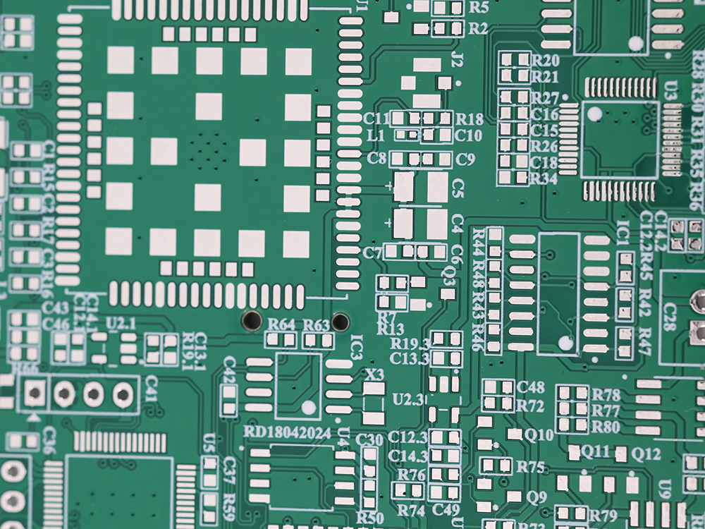
A number of physical and electrical properties define simply exactly how a PCB trace acts. These include trace dimension, trace density, trace size, trace spacing, trace geometry, and surface area finish. With each other, these residential properties determine simply how much existing the trace can carry, just how much resistance it has, and just how conveniently it can move a signal.
Trace size is the straight size of the copper path. Broader traces can lug a lot more existing and run cooler. Slim traces offer for thick directing, yet they could not be suitable for high-voltage line.
Copper density is frequently specified using copper weight or microns. Thicker copper lowers resistance and enhances thermal performance. This is why PCB copper weight is a vital part of PCB trace current ability estimations.
Lengthy traces have extra resistance and even more possibility for signal hold-up. In digital or RF boards, trace size can impact timing, insusceptibility, and sound.
Spacing in between traces helps avoid crosstalk and EMI. Not enough spacing can allow signals to hinder each other, especially in high-speed PCB layout.
Sharp corners, extreme bends, and negative transferring angles can create issues. A great deal of engineers pick 45-degree sending due to the reality that it is cleaner for manufacture and usually much better for signal routines than sharp 90-degree turns.
Vias attach layers in multilayer boards. They serve, nonetheless each via includes a small amount of resistance and inductance. That matters in high-speed or high-current styles.
Trace performance likewise relies on the ending up layer and how well the copper is secured throughout PCB fabrication and PCB establishing. A trace that is subjected or incorrectly completed may be much less reliable or harder to solder.
|
Property |
Effect on PCB Performance |
|
Width |
Current ability, warmth, resistance |
|
Thickness |
Lower resistance, far better present handling |
|
Length |
More resistance, even more delay |
|
Spacing |
EMI and crosstalk control |
|
Geometry |
Fabrication top quality and signal practices |
|
Vias |
Layer transitions and directing convenience |
PCB trace current is the quantity of electrical existing streaming using a copper trace. This might seem apparent, yet it is simply one of the most crucial design variables in a board. If a trace lugs extra existing than it was made for, it can get too hot, lose voltage, or fall short entirely. That is why designers compute present bring capability prior to completing the design.
The present a trace can lug relies on:
Trace size
Copper density
Trace dimension
Ambient temperature level
Permitted trace temperature level
Cooling issues
Board material
A larger trace can carry a great deal much more current as a result of the truth that it has more cross-sectional location. A thicker copper layer additionally helps becuase it decreases resistance. In contrast, an extensive slim trace has much less current-carrying ability and is probably ahead to be hot.
Existing impacts:
Power distribution
Voltage decrease
Trace temperature
Board dependability
Safety and security
PCB board efficiency
Obtaining also hot
Copper delamination
Melted trace sectors
Open up circuits
Lowered product life span
Solder joint tension
Great PCB directing is not arbitrary. It abides by a plan. Traces should be transferred to keep power and ground secure, secure signal top-notch, and lower disturbance. In practice, this suggests splitting numerous kinds of signals, regulating return courses, and picking the appropriate layer framework.
Keep power traces big and brief
Maintain signal traces clean and straight
Use ground aircrafts to decrease sound
Prevent unneeded loopholes
Separate high-speed signals from low-speed signals
Use vias extensively in important paths
Power traces should certainly normally be bigger than signal traces because they carry a whole lot a lot more existing. Ground planes offer a low-impedance return program and assistance keep the board. Signal traces should certainly be routed to prevent loud locations, specifically near switching regulatory authorities, motors, or RF sources.
|
Routing Method |
Strength |
Weakness |
|
Autorouting |
Fast and convenient |
May create bad trace premium quality |
|
Hands-on routing |
Better control and optimization |
Takes much more time |
Usage 45-degree trace directing
Maintain traces short when feasible
Keep continuous sizes for essential webs
Avoid sharp trace edges
Usage teardrop pads where honesty concerns
Examine routing with design policy monitoring (DRC).
In multilayer PCB design, routing is typically easier due to the truth that signals can relocate between interior layers. However, every using requirement to be utilized actively. Through-hole vias, blind vias, and buried vias each have a different impact on cost and performance.
In high-speed electronics, trace size affects greater than existing. It similarly affects trace insusceptibility, which affects signal representation. If a trace's insusceptibility changes all of a sudden, part of the signal can improve rather than proceeding onward cleanly. That is called reflection, and it can damage signal top quality.
Unexpected trace size adjustments.
Insusceptibility inequalities.
Poor changes in between layers.
Poor adapter directing.
Sharp geometry modifications.
Lengthy unterminated signal lines.
The width of a trace contributes to its electrical qualities. Broader traces typically have reduced insusceptibility, while narrower traces have greater insusceptibility. In high-speed PCB layout, this matters a bargain because of the truth that signals have to move predictably. If the resistance is not taken care of, the result may be calling, timing blunders, or damaged details.
Preserve trace size regular.
Suit resistance where required.
Avoid breakthrough in geometry.
Use ideal discontinuation in high-speed lines.
Keep directing neat and quick.
Different noisy traces from delicate ones.
Signal representation is particularly vital in:.
USB differential sets.
LVDS transmitting.
RF PCB style.
Quick digital buses.
Clock lines.
High-frequency interaction web links.
A circuit card had recurring digital mistakes in a high-speed clock line. The concern was triggered by a trace that changed width suddenly near a port. That little geometry change established depiction. After the trace was upgraded with a continuous size, the mistakes disappeared.
Creating traces well is among the fastest methods to improve board high quality. Excellent trace design helps with thermal safty, signal precision, and generating return. It addionally makes the board much less complicated to examine and deal with later.
Select trace size based on existing.
Utilize bigger traces for power training courses.
Maintain high-speed traces brief and straight.
Keep free from routing delicate signals near loud elements.
Maintain correct trace spacing.
Use a clean ground aircraft.
Apply DRC prior to manufacture.
Use ground places for thermal assistance.
Include decreases for more powerful pad web links.
Route with 45-degree angles.
Use differential collection guiding for balanced signals.
Think about impedance for RF and high-speed lines.
Model and examination prior to final manufacturing.
|
Best Practice |
Benefit |
|
Bigger power traces |
Less warm and reduced resistance |
|
Brief signal paths |
Better signal integrity |
|
Ground planes |
Lower sound and much better return courses |
|
Teardrops |
Stronger trace-to-pad shifts |
|
DRC checks |
Fewer construction mistakes |
|
Differential routing |
Better high-speed balance |
Understanding PCB trace practices is crucial since traces affect virtually every part of board top quality. They influence specifically how the board lugs existing, how much noise it creates, simply just how much warmth it creates, and just exactly how well it can be made. In PCB manufacture, trace width and spacing require to additionally match the production process. If the designer overlooks those standards, the board could be tough or difficult to construct properly.
Trace comprehending issues for:
PCB stability.
PCB existing handling.
PCB thermal outcomes.
PCB signal top quality.
PCB manufacturability.
PCB repairability.
Fabricators appreciate:.
Etching limitations.
Minimum trace size.
Trace spacing.
Copper density.
Layer stackup.
DFM conformity.
Setting up teams appreciate:.
Solderability.
Thermal blood circulation.
Part placing.
Revamp get to.
Board durability.
Developers treatment considering that trace activities influences:.
Voltage stability.
Sound decrease.
Signal honesty.
Element life.
System safty and security.
Make use of a PCB trace size calculator or design formula based upon existing, copper density, temperature level, and enabled voltage decrease.
A microstrip operates an external layer, while a stripline runs in between inner layers. Stripline is generally better shielded.
Trace completes affect just how well solder bonds, exactly how immune the copper is to oxidation, and just exactly how trustworthy the last web link becomes.
Typical reasons consist of overheating, delamination, over-etching, bad directing, crosstalk, and mechanical damages.
They are happening much more impedance-controlled, far more firmly transferred, and far more depending on stackup and simulation.
Start with appropriate trace dimension, maintain courses short, use ground planes, comply with DRC guidelines, and design early.
 Hot News
2026-06-25
2026-06-23
2026-06-15
2026-06-11
2026-06-09
2026-06-06
2026-06-03
2026-05-31