Quick Links
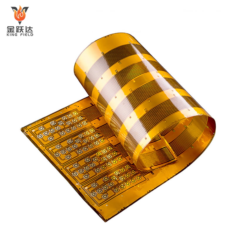
A Twin Inline Bundle (DIP) is amongst among one of the most well-known and historically important IC packaging styles in electronics. It is a timeless through-hole package that utilizes two similar rows of pins to connect an incorporated circuit to a released circuit board (PCB). Although modern-day digital devices frequently depend on smaller surface-mount modern technology (SMT) components, the DIP strategy continues to be important since it is easy to solder, straightforward to change, and truly helpful in PCB prototyping, education and learning, repair, and low-volume production. If you have in fact ever taken advantage of a breadboard, set up a do it yourself circuit, or collaborated with older electronics, you have actually potentially seen a DIP chip in activity.
Identifying what is a Twin Inline Plan serves for any individual involved in digital tools format, repairing, prototyping, or production. It assists you make smarter options when selecting bundle kinds for bundled circuits (ICs), memory chips, logic chips, microcontrollers, and various other electronic elements. It furthermore offers you a much better structure for contrasting DIP vs SMD, DIP vs SOP, DIP vs QFP, and DIP vs BGA.
A DIP is not simply a form. It is an item packaging approach with details concessions. Its larger dimension can be a negative aspect in mobile products, yet that similar dimension makes it less complex to solder by hand and simpler to examine on a breadboard. Its through-hole leads are mechanically solid, but they also use up added board room than modern surface-mount strategies. That balance is precisely why DIP is still commonly made use of in electronic gadgets prototyping, commercial electronics, training electronic tools kits, and tradition systems.
Imagine you are constructing a tiny prototype circuit for an university job or checking out an amplifier design on a breadboard. A DIP component is a lot easier to place, swap, and solder than a small surface-mount chip. You do not require ingenious reflow equipment or tiny assessment tools. You can simply put the chip, confirm the DIP alignment, solder the pins, and evaluate the circuit. That kind of ease is amongst the largest factors the Double Inline Bundle stays vital.
Even in a globe of SMT technology, portable IC item packaging, and high-density PCB applications, DIP still supplies an actual goal. It is especially handy where:
Hand-operated soldering is chosen
Repairings need to be basic
Parts require to be altered generally
Cost problems greater than measurement
Developers desire a plan that functions well on a PCB prototype
A Twin Inline Bundle (DIP) is a type of digital component plan used to house an integrated circuit or other semiconductor device. It is called "double inline" because it has 2 parallel rows of pins extending from contrary sides of the rectangle-shaped package body. Those pins are put right into openings in a PCB, which is why DIP is described as a through-hole package. In basic electronics language, a DIP is a strategy that makes an IC very easy to area, solder, and connect to a circuit card. Because of that, the DIP strategy turned into one of one of the most favored type of IC product packaging in the very early days of modern electronic devices.
The primary function of a DIP is to offer both electrical link and mechanical support. The IC inside the plan is the real semiconductor tool, however the DIP body secures it and provides developers a beneficial technique to install it on a board. The pins are arranged in a standard pattern so they can be used in PCB establishing, breadboards, outlets, and examination fixtures. This is why DIP is normally referred to as a breadboard-compatible IC plan or a socket-compatible layout. It is not only a technique to hold a chip-- it is a method to make the chip valuable in real circuit designs.
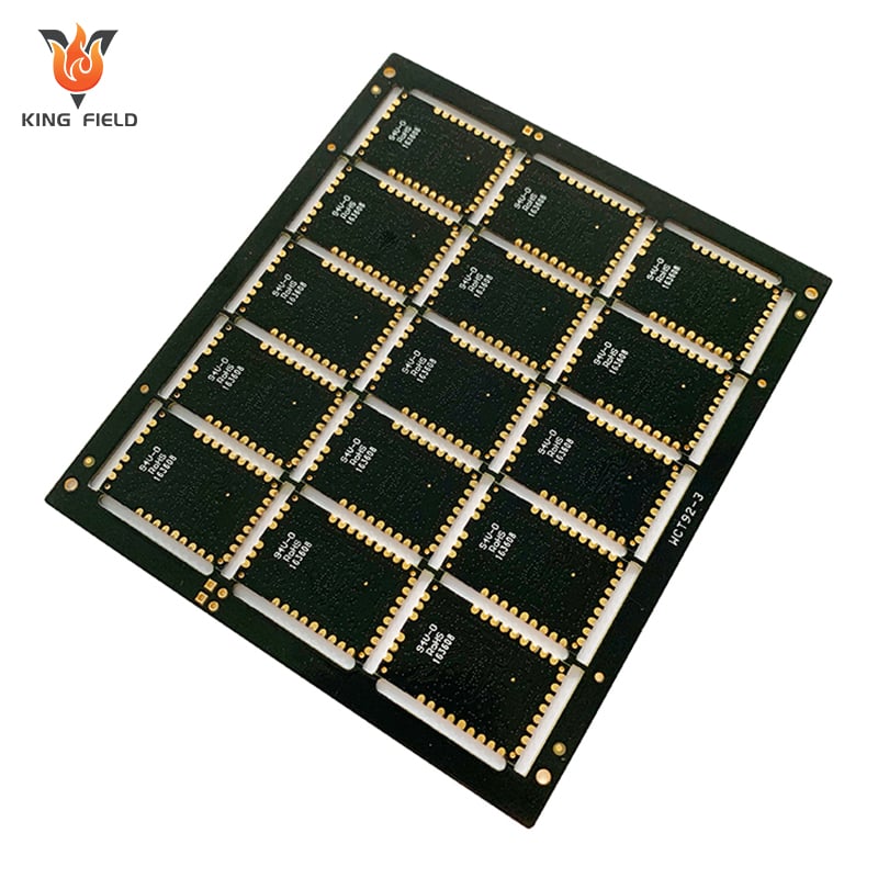
DIP strategies are commonly associated with the DIP chip, DIP IC, or Double In-line Bundle IC. They can be found in several pin counts, such as DIP8, DIP14, DIP16, and larger versions. The number after "DIP" commonly explains the pin matter. As an example, a DIP16 plan has 16 pins full, with 8 pins on each side. This standard method makes it simple for designers to understand pin configuration, pin spacing, and board design demands. For the most part, the pin pitch is 2.54 mm (0.1 inch), which is furthermore the conventional spacing used in a number of breadboards and version boards.
In electronic devices, DIP definition is basic:
Double = two rows
Inline = pins straightened out in rows
Plan = the figure that houses the chip
|
Feature |
Description |
|
Package body |
Rectangular plastic or ceramic covering |
|
Pin rows |
Two parallel rows of steel leads |
|
Placing style |
Through-hole setting up |
|
Usual use |
ICs, reasoning chips, memory chips, switches, screens |
|
Setting up method |
Manual soldering or automated through-hole insertion |
|
Common pitch |
2.54 mm in between pins |
DIP happened liked as a result of the fact that it settled countless early electronics troubles at the same time. It used designers a reputable method to place chips on a printed motherboard, it was really easy to inspect visually, and it was straightforward to solder by hand. It also functioned well with the manufacturing devices available at the time. Subsequently, DIP became a typical PCB package in consumer electronic devices, business electronic devices, and computer systems for years.
An added factor for its allure is that DIP is extremely beginner-friendly. If you are learning electronics, managing a DIP plan is generally easier than handling small SMT parts. The pins are significant enough to see and touch, and the part can be set up without cutting-edge surface-mount devices. That is why DIP stays a liked in electronics prototyping, do it yourself circuit format, and academic sets.
Today, numerous modern gadgets utilize SOP bundles, QFP, TQFP, or BGA given that those strategy makes assistance smaller sized effects and greater pin thickness. However these strategies are generally tougher to solder by hand and more challenging to evaluate in simple lab conditions. DIP remains useful due to the fact that it is straightforward, tough, and easy to collaborate with, especially for low-volume or educational applications.
Despite the fact that contemporary electronic devices increasingly make use of smaller sized packages, the term Double Inline Plan is still vital since it clarifies an extremely details bundle style with real design results. When a designer sees DIP, they swiftly understand:
the plan makes use of through-hole pins,
the board ought to have matching openings,
the strategy is most likely very easy to hand-solder,
and the element might be simpler to change later.
A DIP strategy features by connecting the interior integrated circuit to the outdoors board through its pins. The IC inside the strategy refines signals, and the pins provide the physical course for those signals, plus power and ground. As soon as taken into a PCB, each pin gets in a pierced opening and is soldered on the contrary side of the board. This is why DIP is taken into account a through-hole development bundle. The electrical link is created via the metal opening plating and solder joint, producing a secure mechanical and electric bond.
The pins are the primary user interface betwen the chip and the outdoors curcuit. Some pins bring input signals, some bring result signals, some lug power, and some are used for ground or control functions. Oftentimes, the bundle pinout is basic to make design and substitute simpler. For example, a reasoning IC in a DIP16 package might have certain pin tasks for VCC, GND, inputs, and results. Designers need to understand the pinout prior to putting the bundle on the board since the feature of each pin is essential to circut procedure.
The method DIP works is very closely connected to PCB soldering and digital motherboard setting up. As soon as the pins travel via the board, solder is related to produce a risk-free connection. This through-hole link is one factor DIP is recognized for mechanical stamina. The solder joint and the pin together develop a robust bond that withstands drawing and resonance far better than various surface-mount components. That makes DIP helpful in applications where the element may be taken care of regularly or where toughness matters more than density.
A routine DIP chip could consist of pins for:
Power
Ground
Input signals
Result signals
Clock
Enable or reset
Address or information lines
The process normally consists of:
Straightening the package with the PCB openings
Putting the pins via the holes
Turning the board
Soldering the pins
Cutting excess lead size if needed
Examining the solder joints
DIP is a through-hole package, which suggests the pins take a trip with the PCB. This varies from surface-mount gizmos (SMD), which sit on top of the board and are soldered to surface pads. Through-hole installing generally provides far better mechanical assistance, while SMT sustains greater density and automation.
|
Feature |
DIP Through-Hole |
SMT Package |
|
Board connection |
Pins take a trip through holes |
Components hinge on the area |
|
Mechanical strength |
High |
Moderate |
|
Setting up speed |
Slower by hand |
Faster in automation |
|
Alleviate of repair |
Easier |
Harder for little components |
|
Board density |
Lower |
Higher |
Installing a DIP plan is among the most convenient tasks in digital tools setting up, which is a significant part of why it continues to be so famous. Considering that DIP uses through-hole placing, the pins are put right into pierced holes in the PCB before soldering. This establishes stable electrical contact and mechanical fixation.In many cases, the part can similarly be placed into a DIP socket, which enables it to be done away with later on without desoldering. That makes installation, testing, and substitute much easier than with various surface-mount packages.
The common setup procedure begins with checking out the DIP positioning. The majority of DIP packages have a notch or dot noting pin 1, which helps quit reversed setup. When the chip is straightened with the holes, the pins are very carefully placed. If the board uses a socket, the socket is firm initially and the chip is put later. If the chip is soldered right, the strategy is placed with the board and solder is applied to the in contrast side. After soldering, the joints are inspected completely wetting, ideal form, and safeguarded add-on.
DIP installment is specifically beginner-friendly due to the fact that it does not need reflow stoves, stencil printing, or fine-pitch positioning tools. Standard devices are enough:
Blowpipe
Solder
Adjustment
Tweezers or tiny pliers
PCB or breadboard
Multimeter
Desoldering devices if needed
A DIP outlet makes setup and replace a great deal much easier. In contrast to soldering the chip directly to the board, the outlet is firm at first. Afterwards the IC is linked into the outlet later on. This serves for:
Prototyping
Regular chip replacement
Reprogramming or testing
Safeguarding heat-sensitive ICs
Repair-friendly designs
The Double Inline Plan is still typically made use of in applications where simplicity of use, toughness, and serviceability are more important than ultra-compact size. It is especially common in digital devices that are easy, instructional, low-volume, or legacy-based. Because DIP strategies are straightforward to manage and solder, they are impressive for PCB prototyping and rookie work. They are likewise helpful in older customer tools, industrial control systems, and examination tools.
Integrated circuits
Reasoning ICs
Op-amps
Memory chips
Microcontrollers
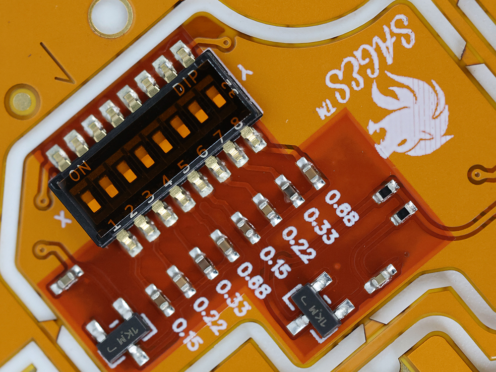
DIP switches
Hand-operated setup setups
Tool choices and attending to
LEDs and seven-segment screen elements
Indication lights
Numerical display screens
Relays
Control circuits
Switching applications
Educational electronic devices sets
Class use
Laboratory training
Do it yourself electronic tools and breadboard projects
Leisure activity circuits
Prototyping
Retro electronic devices repair work service
Timeless computer systems
Audio gadgets
Heritage commercial systems
DIP serves beacuse it is:
Easy to place and change
Appropriate with firm or socket-mounted designs
Strong adequate for through-hole use
Fundamental to analyze and fix
Affordable for straightforward circuits
Many classic DIP microcontroller and thinking devices are still used in training research laboratories and prototyping boards. This is due to the fact that the plan makes the chip easy to link to breadboards and model PCBs. Designers can rapidly inspect a circuit, modification well worths, or switch over out a chip without needing sophicated SMT gadgets.
Contrasting DIP vs SOP packages, DIP vs QFP, and DIP vs BGA aids describe why DIP is still made use of and where it fails. Each bundle type addresses a diffrent design trouble. DIP is older, bigger, and much less made complex to take care of. SOP and QFP are smaller sized and much better for modern-day PCB thickness. BGA sustains very high pin matters and effectiveness, yet it is a lot harder to examine and rework. That makes DIP one of the most readily available strategy and BGA among the most advanced.
A SOP package is a surface-mount style strategy that is smaller sized and more suitable for computarized establishing. It preserves area on the PCB and operates well in little products. DIP, comparative, is bigger and much easier to solder by hand. The primary tradeoff is that SOP supports greater thickness, while DIP supports much less difficult prototyping and repair work solution.
A QFP or TQFP plan places pins on all 4 sides and sustains a much greater pin count in a smaller effect. It prevails in modern electronic devices, specifically where board area is restricted. DIP is much easier to set up, yet QFP is far better for small gadgets and advanced electronics.
A BGA package uses solder rounds under the component rather than subjected pins. It is suitable for high-density, high-performance chips, yet it calls for cutting-edge assessment and redesign techniques. DIP is a whole lot less complicated to handle, yet it can not match BGA in pin density or board-space efficiency.
Despite the fact that modern strategy kinds are much more space-efficient, DIP still has advantages:
Best for hand assembly
Easy to examine cosmetically
Easy to use in breadboards
Helpful for low-volume production
Strong through-hole mounting
Choosing the ideal bundle relies on the item's goals. If the job is a prototype, a DIY build, or a fixing task, DIP may be the most effective choice. If the style should be portable, high-density, and mass-produced, SMT packages are usually better. This is why package option is not only a technical decision but additionally a business one. The most effective plan is the one that fits the product's phase, spending plan, and reliability needs.
Usage DIP when you need:
Easy hand soldering
Easy substitute
Breadboard compatibility
Simple testing
Low-volume manufacturing
Teaching and finding out applications
Use SMT when you require:
Smaller footprint
Higher part thickness
Automated mass production
Better use PCB area
More advanced customer electronics layout
The major advantages are easy hand soldering, great mechanical strength, easy examination, affordable, and compatibility with breadboards and outlets.
The common pin pitch is usually 2.54 mm (0.1 inch), with common row spacing around 7.62 mm for typical DIP layouts.
It connects an interior IC to a PCB via 2 rows of pins that are put right into holes and soldered on the contrary side of the board.
SIP features a single pin row, whereas DIP comes with two parallel pin rows
Typical tools consist of a soldering iron, solder, tweezers, PCB or breadboard, desoldering devices, and a multimeter.
 Hot News
2026-06-25
2026-06-23
2026-06-15
2026-06-11
2026-06-09
2026-06-06
2026-06-03
2026-05-31