Quick Links
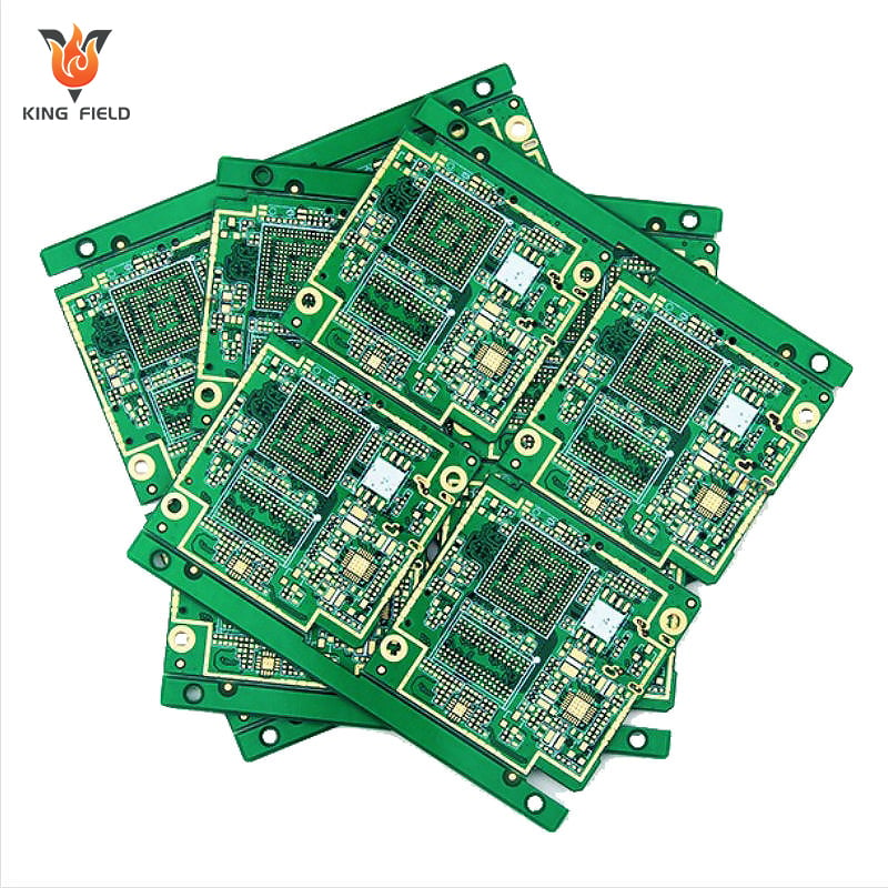
Chip aboard (COB) is among one of one of the most vital PCB packaging modern technologies in modern-day digital devices as a result of the fact that it assists programmers create smaller, quicker, and added thermally dependable items. At its core, COB development recommends attaching a bare semiconductor die directly onto a PCB substratum or different olther installing surface rather than positioning the chip inside a different plastic or ceramic bundle originally. This direct chip mounting method is what makes COB product packaging so enticing in portable digital tools, LED lights, customer electronic tools PCB styles, and lots of type of high-performance PCB assemblies. In a world where things are anticipated to be thinner, lighter, and a lot more powerful, COB has actually come to be a valuable method for digital miniaturization and PCB efficiency optimization.
The reason COB is so extensively used is fundamental: it resolves a variety of concerns at the same time. Originally, it lowers dimension by removing the demand for additional product packaging around the chip. Second, it boosts signal stability becasue the electrical program in vetween the semiconductor pass away and the motherboard is much shorter. Third, it sustains far better thermal surveillance PCB effectiveness given that warm can transfer much more straight right into the substrate and much from the energetic tool. 4th, it can decrease generating price in high-volume production by lowering product packaging actions and streamlining part matter. For a number of engineers and makers, that mix of space-saving electronics, signal loss decrease, and cozy dissipation modern technology makes COB an incredibly beneficial alternative for cutting-edge PCB setting up and digital product packaging alternatives.
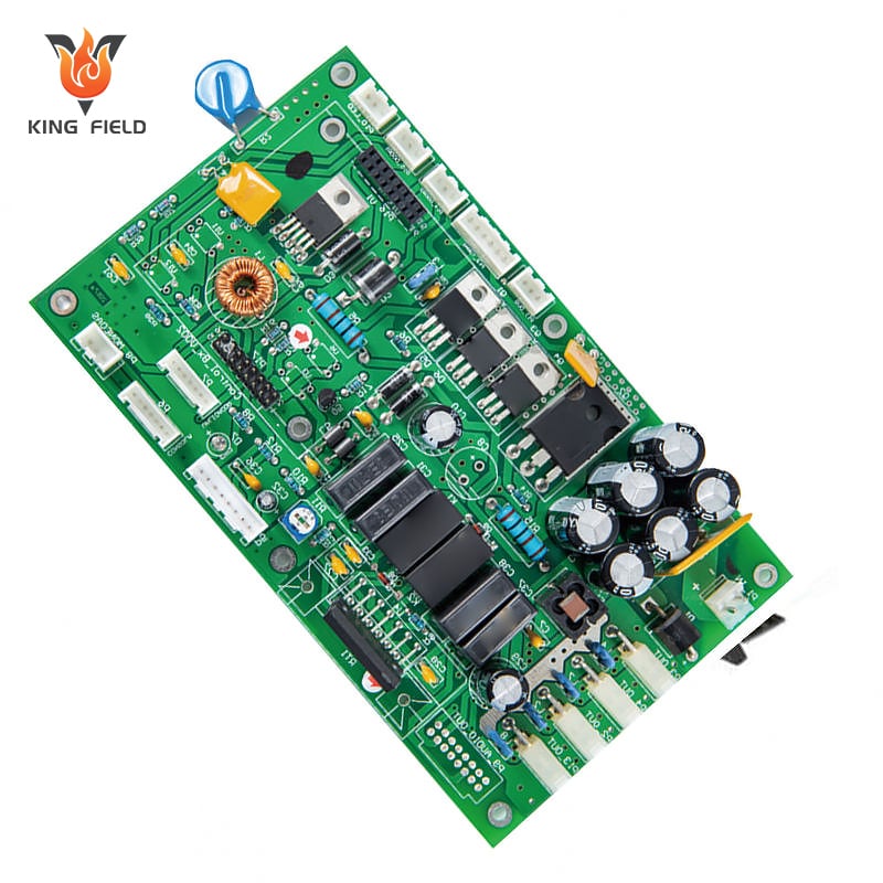
COB is particularly important in industries where integrity and small dimension both matter. In LED lights PCB systems, COB LED frameworks provide high lumen density and effective warmth circulation. In car PCB assemblies, COB can assist assistance sensing device parts, control parts, and lights systems that need to endure vibration, temperature level swings, and wetness direct exposure. In medical PCB and aerospace PCB styles, COB might be taken advantage of when designers desire sophisticated item packaging with outstanding electrical efficiency and tighter board combination. In RF
PCB applications, the decreased parasitic influences of bare die placing can enhance high-frequency practices. That is why Chip aboard product packaging is not just a particular niche technique-- it is a considerable manufacturing approach made use of across many areas of the digital devices making market.
Chip aboard (COB) is a semiconductor item packaging approach where a bare silicon die is installed straight onto a PCB substratum or various other base product. Instead of positioning the chip inside a completed plastic bundle first, the manufacturer connects the chip itself to the board and after that affixes it utilizing cable television bonding, flip-chip technology, or different other PCB assembly methods. This is why COB is typically described as straight chip mounting or bare die placement. It gets rid of extra item packaging layers, which can increase electrical conductivity, save room, and make the end item additional reputable.
The core idea behind COB technology is very useful: location the chip as close as feasible to the circuit that supports it. The shorter that connection path is, the much less chance there is for signal loss, parasitic capacitance, unfavorable inductance, or unnecessary warmth accumulation. In high-speed and high-density designs, those tiny improvements matter a great deal. COB is one reason several portable electronic devices can be smaller sized without quiting excessive performance. It also helps manufacturers establish high-density packaging solutions for devices that require to do more in much less room.
COB differs from traditional incorporated circuit product packaging beccause it gets rid of the protective bundle around the die at the start of the setting up flow. That indicates the chip is subjected throughout production, so the procedure calls for excellent PCB quality assurance, exact tooling, and strong environmental management afterward. In a number of styles, the die is safeguarded with epoxy product covering, silicone encapsulation, or conformal layer to prevent dampness, dirt, vibration, and mechanical problems. This is one element COB is normally made use of in products that maintain thickness with stability.
|
Feature |
COB |
Traditional Packaged IC |
|
Chip form |
Bare die |
Pre-packaged chip |
|
Setting up method |
Directly on PCB or substrate |
Mounted as a packaged part |
|
Size |
Smaller |
Larger |
|
Signal path |
Shorter |
Longer |
|
Heat transfer |
Better in numerous designs |
Less direct |
|
Repairability |
Harder |
Easier |
|
Setting up complexity |
Higher precision required |
Easier handling |
COB contemporary innovation is made use of whenever designers want a smaller, extra efficient, and often extra thermally regulated means to package semiconductors. Its use is particularly usual in items where space-saving digital gadgets and high-performance PCB demands overlap. Due to the fact that the chip is mounted directly onto the board, COB can help reduce influence while increasing signal stability and lowering some types of electrical disturbance. That makes it a strong selection for products that require both miniaturization and strong efficiency.
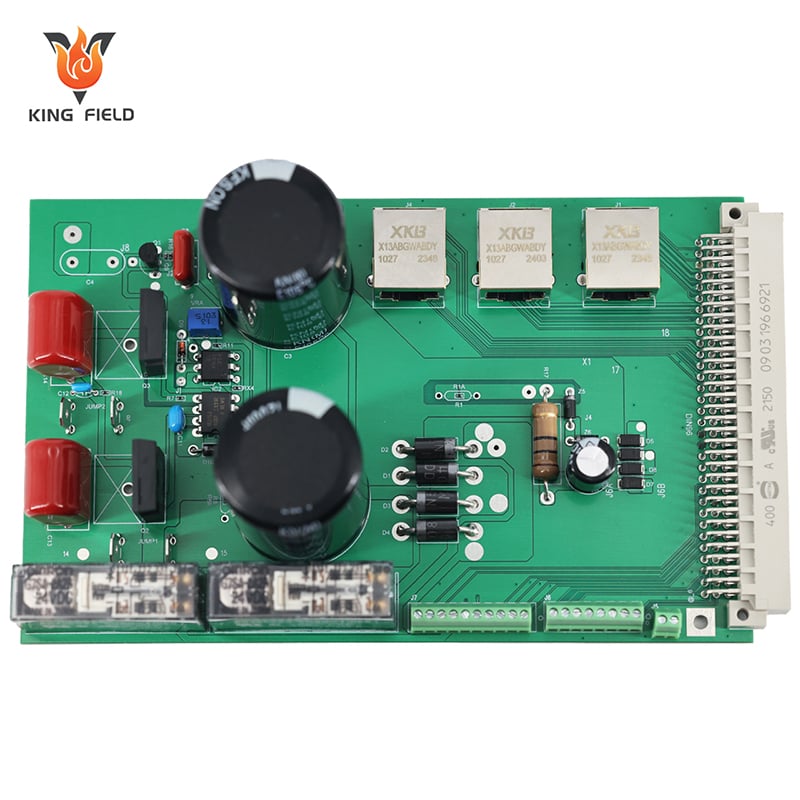
Among the best factors COB is used so widely is that it adjusts well to various markets. In customer electronic devices PCB design, COB can aid producers make phones, wearables, and smart gadgets smaller sized and lighter. In business electronic devices, it can sustain control modules and sensor systems that need stable treatment in hard ambiences. In automobile PCB products, COB can assist with tiny picking up device parts, lighting systems, and control devices. In RF PCB styles, it can enhance high-frequency habits by lowering parasitical results and reducing trace sizes.
COB furthermore plays a significant function in LED illumination PCB applications. COB LED structures placed several light-emitting chips directly on a substratum to develop high lumen thickness and effective warm flow. This is why COB LED items are frequently located in spotlights, commercial lights, building lighting, and high-output parts. The contemporary innovation sustains much better warm dissipation advancement and can increase consistent brightness. Simply put, COB is not just regarding electronic devices-- it is in addition a significant item packaging strategy for modern lighting.
Customer electronic devices PCB
Smart tools
Wearables
Smart home tools
IoT boards
LED lighting PCB
High-output lights
Commercial lighting
Industrial lights
Automotive PCB
Sensing unit components
Control modules
LED lights systems
Clinical PCB
Diagnostic devices
Compact radar
Aerospace PCB
Avionics electronics
High-reliability components
RF PCB
High-frequency circuits
Signal-sensitive modules
Smaller sized board impact
Better thermal management PCB
Lower signal loss decline
Fewer packaging steps in some layouts
Outstanding ideal for high-density interconnect products.
Practical for ingenious PCB assembly.
The biggest appeal of Chip aboard packaging is that it combines density, performance, and rate benefits in one strategy. By placing the die straight on the board, the design typically becomes smaller and electrically cleaner. That can boost performance in high-speed electronic gadgets, minimized some kinds of signal interference, and help with warmth circulation. These benifits make COB particularly appealing for portable circuit layout, digital circuit miniaturization, and PCB efficiency optimization.
1. Miniaturization
COB is often made use of when developers require to press even more ability right into much less space. By getting rid of the external plan, an item can reduce substantially. In some applications, COB can lower the footprint by 30-- 50% compared to even more normal item packaging strategies. That is a major gain for products like brilliant gadgets, mobile tools, and wearable electronics.
Due to the fact that the chip is installed straight onto the PCB or substratum, the electrical path is much shorter. That implies:.
Much less resistance.
A lot much less inductance.
Less signal hold-up.
Far better signal stability.
Decreased parasitical components.
These improvements are particularly handy for high-frequency applications, signal conditioning circuits, and advanced digital tools packaging.
Cozy is one of the biggest opponents of digital gadgets. COB aids because it can transfer cozy a lot more right into the substrate and surrounding items. This is very crucial for high-power LED product packaging, power electronics, and tiny systems that run constantly. Far better warmth flow suggests lower component anxiousness and far much better long-lasting reliability.
4. Lower Cost
COB can reduce price by getting rid of numerous of the steps associated with usual packaging. Less bundle elements could furthermore show a lot less stock and much less intricate supply chains. For high-volume builds, that can make a considerable difference in general production cost.
5. Design Flexibility
COB can handle:.
Double-sided PCB.
Multi-layer PCB.
Adaptable PCB in details systems.
Personalized substrates.
High-density layouts.
That convenience makes it important for PCB prototyping and high-volume PCB production alike.
|
Advantage |
What It Means in Practice |
|
Smaller sized size |
Enables little electronics |
|
Far better signal performance |
Improves price and lessens noise |
|
Better thermal transfer |
Helps with warmth monitoring. |
|
Reduced bundle cost |
May reduce making price |
|
Much less parasitic effect |
Supports high-frequency practices |
|
High integration |
Useful for advanced electronics |
A COB LED lamp could include numerous LED chips positioned strongly together on one substratum. As a result of the reality that the chips are direct-mounted, the resource of light ends up being extremely dense and effective. That produces brighter result and a lot more even lighting. It similarily boosts thermal surveillance, which assists the light last a lot longer.
The COB manufacturing process is an exact series of actions that transforms a bare semiconductor pass away right into a protected and practical setting up. Unlike common SMD placement, COB requires conscious handling because the chip is exposed and more fragile throughout establishing. The procedure generally consists of substratum prep work, die accessory, wire bonding, encapsulation, and screening. Each action affects the last performance, reliability, and apprearance of the product.
The process starts with preparing the PCB substratum or base product. The surface area needs to be clean, level, and prepared for bonding. Relying on the style, the maker might apply conductive epoxy or an additional glue to produce the base for chip attachment. The substratum item is picked based upon thermal, electric, and mechanical needs.
Next off, the bare die is placed onto the substratum making use of a pick-and-place manufacturer or precision die-bonding gadgets. This step is called pass away accessory or straight die attach. The placing need to be really specific since also small misalignment can influence electric web link or bonding high quality.
After the die is connected, the electrical links are made using cord bonding. Fine cables-- usually gold, copper, or light weight light weight aluminum-- connect the chip pads to the PCB traces or bonding pads. 2 common approaches are:.
Wedge bonding.
Ball bonding.
Cord bonding is one of one of one of the most essential parts of COB establishing because of the reality that it develops the electric bridge in between the semiconductor die and the board.
The adhered chip and cord framework are normally protected with epoxy material covering, silicone, or a glob-top product. This treatment is called encapsulation. It shields the setting up from:.
Moisture.
Dust.
Mechanical anxiety and anxiety.
Vibration.
Managing damages.
When the establishing is overall, it experiences evaluation and testing. Usual approaches consist of:.
Electrical screening.
AOI inspection.
Burn-in testing.
Visual evaluation.
Practical board testing.
These actions aid determine cord problems, gaps, bad adhesive placement, or electric mistakes before the item ships.
|
Step |
Purpose |
|
Substrate preparation |
Create a tidy bonding surface area |
|
Die attachment |
Mount the bare chip |
|
Cable bonding |
Connect chip to board electrically |
|
Encapsulation |
Protect the die and cords |
|
Testing |
Confirm efficiency and stability |
COB production calls for:.
Neat atmospheres.
Specific placement.
Accurate thermal control.
Skilled handling.
Solid quality control.
COB is just one of a number of semiconductor strategy kinds, and it serves to compare it with usual alternatives like BGA, SMD, PoP, and DIP. Each bundle has its strength, yet they resolve different troubles. COB is greatest when portable measurement, thermal control, and straight assimilation matter a great deal of. Various other packages may be better when repairability, standardization, or taking care of benefit are extra crucial.
A BGA bundle makes use of solder spheres to connect a packaged chip to the board. It provides outstanding pin density and defense, and it dominates in CPUs, GPUs, and progressed ICs. COB, comparative, mounts the bare die driectly onto the board.
|
Feature |
COB |
BGA |
|
Chip form |
Bare die |
Packaged chip |
|
Size |
Smaller |
Larger |
|
Protection |
Lower up until encapsulated |
Better built-in defense |
|
Repairability |
Harder |
Also hard, yet additional standard |
|
Regular use |
LEDs, small electronics, RF |
CPUs, memory, progressed ICs |
SMD modern-day technology explains surface mount device setting up, where packaged components are placed on the board. COB can be deemed a much more straight kind of mix.
|
Feature |
COB |
SMD |
|
Packaging |
Direct die |
Packaged components |
|
Warmth dissipation |
Often better |
Depends on package |
|
Assembly |
More specialized |
Easier to automate |
|
Maintenance |
Harder |
Easier |
Package on Strategy (PoP) heaps packaged chips up and down. That works for multifunction devices like smart phones, yet it is various from COB as a result of the truth that COB focuses on straight board-level chip placing.
DIP strategies are older, bigger, and a lot easier to model with. They help standard jobs, yet they do not support the compactness or efficiency of COB.
Comparison Table
|
Package Type |
Best Strength |
Weakness |
|
COB |
Compact, effective, thermally strong |
Hard to take care of |
|
BGA |
High pin issue and protection |
Rework details |
|
SMD |
Easy to automate and handle |
Larger than COB in some cases |
|
PoP |
Vertical integration |
More facility product packaging |
|
DIP |
Simple and basic to use |
Bulky and obsoleted for many modern products |
The largest factor designers pick COB PCB setting up is that it can develop a smaller sized, cleaner, and much more incorporated item. Yet the advantages go beyond size. COB can improve PCB integrity, support far better PCB cozy management, and reduce the variety of item packaging steps in the supply chain. In the best application, it can also lower price and enhance overall product performance.
Main Advantages
Space-saving electronics.
Much better electrical performence improvement.
Improved thermal stress and stress and anxiety resistance.
Lower element elevation.
Minimized parasitic effects.
Strong fit for high-density product packaging.
Great for high-reliability digital tools.
Fewer bundle elements in some styles.
Possibly minimized complete package rate.
Better assimilation with PCB manufacture.
Appropriate for automated and high-volume process.
Much easier to tailor for product-specific demands.
COB can assist:.
Enhance signal rate.
Reduce signal loss.
Support tighter board layouts.
Rise brightness in LED things.
Boost thermal transfer in power-sensitive systems.
For suppliers, COB can maintain:.
Smaller sized product spaces.
Lower product expenses.
A whole lot a lot more budget-friendly product design.
Far better usage board location.
More powerful distinction in little markets.
Chip on Board (COB) is a straight placing and item packaging method that places a bare semiconductor pass away right onto a PCB substratum or other base material. It is commonly made use of considering that it aids items lessen, quicker, and a great deal more thermally reliable. By reducing signal paths and reducing product packaging expenditures, COB sustains signal honesty, thermal management, and little PCB style. That is why it is uncovered in COB LED, consumer electronics, automobile systems, scientific devices, aerospace tools, and RF circuits.
COB is particularly useful when a product requires high-density item packaging and dependable board-level integration. At the same time, it needs careful production, defense, and testing. The procedure consists of substratum preparation, die add-on, cable bonding, encapsulation, and quality control. It is added specialized than basic SMD establishing, but in the appropriate product, the payback is solid.
The significant benefits are smaller dimension, much better thermal behavior, much shorter signal programs, and lowered product packaging complexity in some styles.
Considering that the bare die is installed directly on the substratum, warm should be managed meticulously to stop device stress and anxiety, failing, or performance loss.
Can COB assemblies be fixed?
Frequently, yet fixing service is hard since the die is placed right on the board and normally enveloped after bonding.
COB is finest for portable devices, LED lighting, RF circuits, lorry components, professional electronics, and various other high-density systems.
No. COB LED is a particular application of COB innovation in lighting. COB modern technolgy itself is made use of a whole lot more typically in electronics product packaging.
 Hot News
2026-06-25
2026-06-23
2026-06-15
2026-06-11
2026-06-09
2026-06-06
2026-06-03
2026-05-31