Heavy Copper PCB
With over 20 years of experience in PCB prototyping and manufacturing , KING FIELD prides itself on being your best business partner and close friend, meeting all your PCB needs.
☑ 20+ years of PCB manufacturing experience
☑ DIP daily production capacity 1.5 million points
☑ 12-layer ultra-thick copper plate, high current, matte green ink.
Description
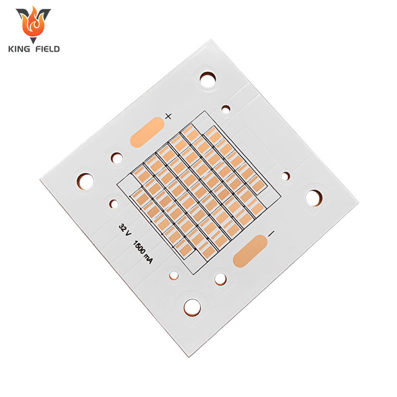
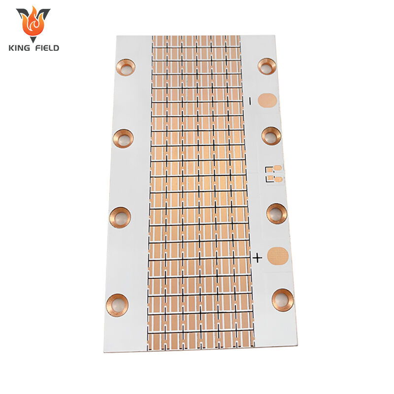
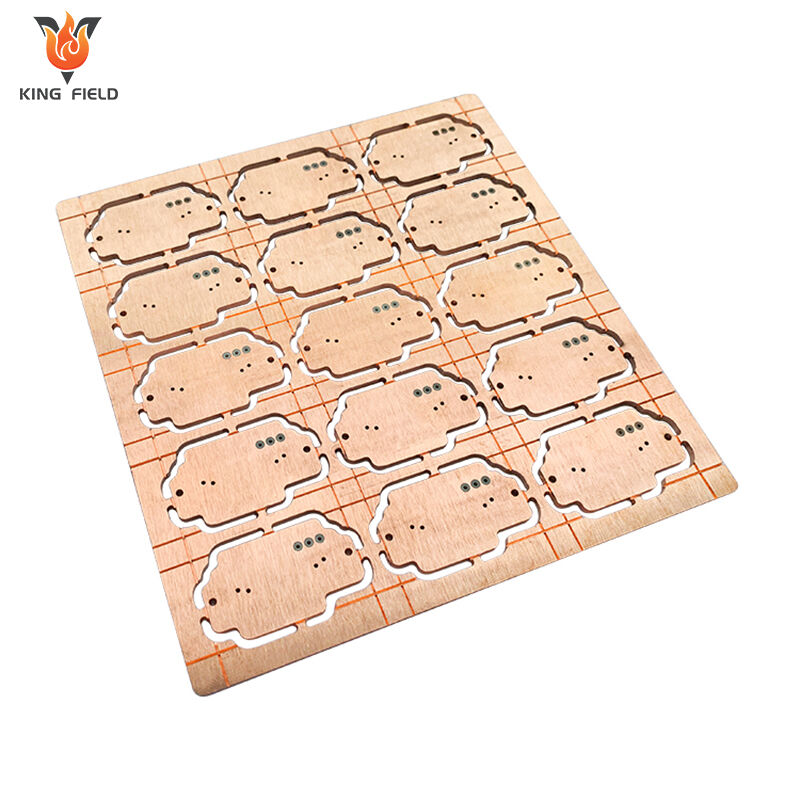
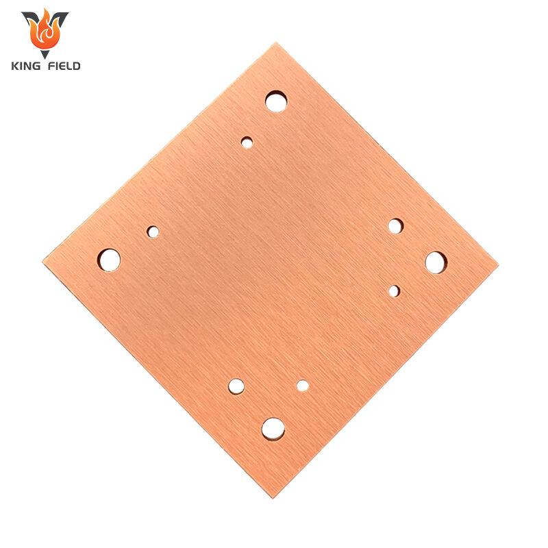
Thick copper PCB
Material: FR4
floors : 12
Process: Sinking Gold
Minimum drilling depth: 0.5mm
Outer copper foil: 6 oz
Inner copper foil: 3 oz
Plate thickness: 4.0mm
What is a thick copper circuit board?
Thick copper circuit boards are a special type of printed circuit board with a copper layer thickness that far exceeds that of standard circuit boards . Generally, the copper thickness of a finished thick copper PCB is ≥2oz . Thick copper PCBs are mainly used in high-power power supplies, automotive ECUs, photovoltaic inverters, and other applications that require high current carrying capacity or efficient heat dissipation .
KING FIELD Thick Copper PCB Manufacturing Parameters
Project |
Ability |
Substrate: |
FR4 , Shengyi S117 0 |
Dielectric constant: |
4.3 |
Outer copper foil thickness: |
6 oz |
Surface treatment method: |
Sinking Gold |
Minimum line width: |
1.0MM |
Application areas: |
Car power supply |
Shelves: |
12 floors |
Plate thickness: |
4.0mm |
Inner copper foil thickness: |
3 oz |
Minimum aperture: |
0.5mm |
Minimum line spacing: |
1.0mm |
Features: |
12-layer ultra-thick copper plate, high current, matte green ink. |
Why choose KING FIELD as your thick copper PCB manufacturer?
l 20+ years of experience in thick copper PCB manufacturing
Founded in 2017, KING FIELD's core team has focused on the PCBA field for over 20 years. As a high-tech enterprise specializing in one-stop PCBA manufacturing, we are committed to "creating an industry benchmark for ODM/OEM PCB intelligent manufacturing" and strive to improve the quality of our products for our customers.
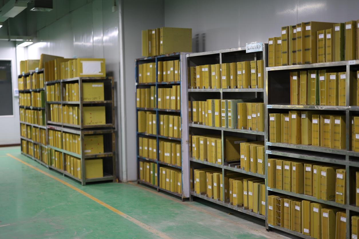
- Scale & Production Capacity
- We own our own surface mount technology (SMT) factory, equipped with a Class 10,000 cleanroom and dedicated medical production lines. The factory covers a total area of over 15,000 square meters and can realize integrated production from SMT placement and THT insertion to complete machine assembly.
-
KING FIELD's production line is equipped with 7 SMT lines, 3 DIP lines, 2 assembly lines, and 1 painting line.
The pin-point YSM20R mounting accuracy is ±0.035mm, and it is capable of mounting the tiniest 01005 component.
Its daily SMT throughput is 60 million points, while its daily DIP output is 1.5 million points.
Response time for urgent orders is 24 hours delivery, meeting customer demands quickly.
l Comprehensive testing and quality assurance
- KING FIELD is equipped with a flying probe tester, 7 automated optical inspection (AOI) units, X-ray inspection, functional testing and other complete testing systems to achieve full-process quality control.
- In terms of quality control, our company has passed six major system certifications: IATF 16949, ISO 13485, ISO 9001, ISO 14001, ISO 45001, and QC 080000. We use a digital MES system for full traceability to ensure that every PCBA is of consistent quality.
l Minimum order quantity for thick copper PCBs
delivery time from prototyping to mass production of thick copper PCBs.
- Prototyping: 24-72 hours
- <20 items : 3-5 business days
- 20-100 items : 5-7 business days
- 100-1000 pieces: 10 business days
- >1000 units: Based on the bill of materials
- After-sales service
KING FIELD also offers an industry-rare "1-year warranty + lifetime technical support" service. We guarantee that if a product suffers from a quality issue that is not caused by the customer, it is eligible for return or exchange free of charge, and we shall cover the associated logistics costs.
- The after-sales team's average response time is no more than 2 hours.
- Problem resolution rate exceeded 98%
FAQ
Q1 : How do you avoid over-etching?
KING FIELD: We use a high-concentration acidic etching solution to quickly remove copper thickness and perform laser trimming on critical signal lines to clean up any remaining burrs .
Q2 : How do you prevent rough hole walls and nail head effect when drilling thick copper plates?
KING FIELD : We use radio frequency plasma to remove resin residue from the hole walls , and then use alkaline permanganate for micro-etching to ensure smooth and defect-free hole walls.
Q3 : How do you address the risks of insufficient adhesive flow and delamination?
KING FIELD: We add fiberglass pads to the thick copper areas for cushioning , and then use deformable steel plates to compensate for thickness differences, ensuring sufficient interlayer filling and strong bonding.
Q4 : How do you ensure the uniformity of copper thickness and adhesion inside the holes?
KING FIELD: We use pulse electroplating , followed by activation with oxygen plasma , and optimize the micro-etching process using a sodium persulfate + sulfuric acid system .
Q5 : What substrate do you usually use for your thick copper PCBs ?
KING FIELD: Thick copper PCBs have high requirements for the substrate. We generally use high TG FR4 as the substrate for thick copper PCBs. Of course, we will also provide material selection solutions based on your copper thickness and number of layers.

